JAJSDS2A September 2017 – February 2022 TIC10024-Q1
PRODUCTION DATA
- 1 特長
- 2 アプリケーション
- 3 概要
- 4 Revision History
- 5 Pin Configuration and Functions
- 6 Specifications
- 7 Parameter Measurement Information
-
8 Detailed Description
- 8.1 Overview
- 8.2 Functional Block Diagram
- 8.3
Feature Description
- 8.3.1 VS Pin
- 8.3.2 VDD Pin
- 8.3.3 Device Initialization
- 8.3.4 Device Trigger
- 8.3.5 Device Reset
- 8.3.6 VS Under-Voltage (UV) Condition
- 8.3.7 VS Over-Voltage (OV) Condition
- 8.3.8 Switch Inputs Settings
- 8.3.9 Interrupt Generation and INT Assertion
- 8.3.10 Temperature Monitor
- 8.3.11 Parity Check And Parity Generation
- 8.3.12 Cyclic Redundancy Check (CRC)
- 8.4 Device Functional Modes
- 9 Programming
- 10Application and Implementation
- 11Power Supply Recommendations
- 12Layout
- 13Device and Documentation Support
- 14Mechanical, Packaging, and Orderable Information
11 Power Supply Recommendations
There are two supply input pins for the TIC10024-Q1: VS and VDD. VS is the main power supply for the entire chip and is essential for all critical functions of the device. The VS supply is designed to be connected to a 12-V automotive battery (through a reverse blocking diode) with nominal operating voltage no greater than 16V. The VDD supply is used to determine the logic level on the SPI communication interface, source the current for the SO driver, and sets the pull-up voltage for the /CS pin. It can also be used as a possible external pull-up supply for the /INT pin as an alternative to the VS supply and it shall be connected to a 3 V to 5.5 V logic supply. Removing VDD from the device disables SPI communications, but does not impact normal operation of the device.
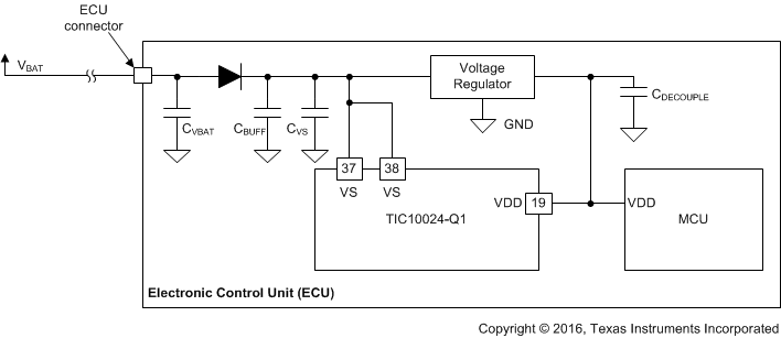
To improve stability of the supply inputs, some decoupling capacitors are recommended on the PCB. Figure 11-1 shows an example on the on-board power supply decoupling scheme. The battery voltage (VBAT) is decoupled on the Electronic Control Unit (ECU) board using a large decoupling capacitor (CBUFF). The diode is installed to prevent damage to the internal system under reversed battery condition. CVS shall be installed close to the TIC10024-Q1 for best decoupling performance. The voltage regulator provides a regulated voltage for the digital portion of the device and for the local microcontroller and its output is decoupled with CDECOUPLE. Table 11-1 lists recommended values for each individual decoupling capacitor shown in the system diagram.
| CRC RULE | VALUE |
|---|---|
| CBUFF | 100 μF, 50 V rated, ±20% |
| CVBAT | 100 nF, 50V rated, ±10%; X7R |
| CVS | 100 nF, 50 V rated |
| CDECOUPLE | 100 nF~1 μF |
 Figure 11-1 Recommended Power Supply
Decoupling