JAJSHF6A May 2019 – August 2020 TMP390
PRODUCTION DATA
- 1 特長
- 2 アプリケーション
- 3 概要
- 4 Revision History
- 5 Pin Configuration and Functions
- 6 Specifications
- 7 Detailed Description
- 8 Application and Implementation
- 9 Power Supply Recommendations
- 10Layout
- 11Device and Documentation Support
- 12Mechanical, Packaging, and Orderable Information
7.3.2 Trip Test
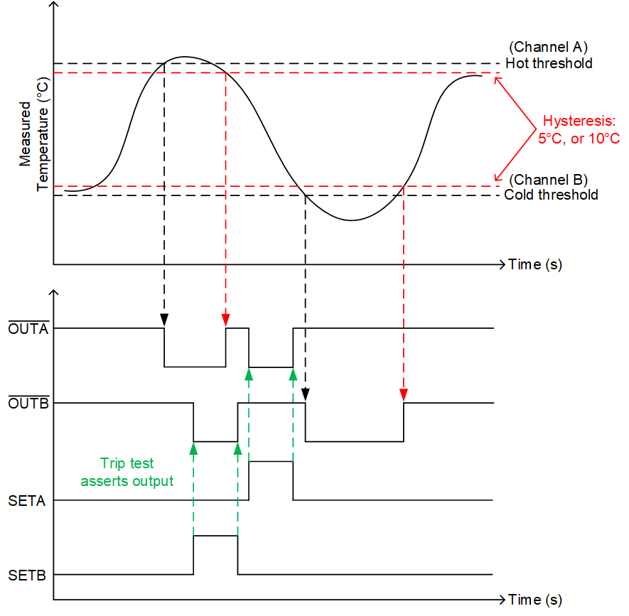
The purpose of the trip test is in system manufacturing test without putting the TMP390 through costly temperature verification of the assembly of TMP390 and pullup resistors. When the SETA or SETB pin is set to a high logic level, the associated output goes low. When the input pin level goes low, the output goes to its previous condition before the trip test. The trip test does not affect the current condition of the device. The trip test signals should stay above 0.8 × VDD for logic high and below 0.2 × VDD for logic low.
The trip test operation is shown in Figure 7-2. The trip test must be performed with a single toggle when the device is operating at a temperature that will not cause the corresponding output to trip. The trip test is intended for production testing after assembly, and must not be used as a functional feature.
 Figure 7-2 TMP390 Trip Test Operation