SBAA229B april 2017 – june 2023 AMC1100 , AMC1200 , AMC1200-Q1 , AMC1211-Q1 , AMC1300 , AMC1300B-Q1 , AMC1301 , AMC1301-Q1 , AMC1302 , AMC1302-Q1 , AMC1311 , AMC1311-Q1 , AMC1411 , AMC1411-Q1 , AMC3301 , AMC3301-Q1 , AMC3302 , AMC3302-Q1 , AMC3330 , AMC3330-Q1 , ISO224 , TLV170 , TLV6001
Introduction
Whether you are sensing current in an industrial 3-phase servo motor system, a battery management system for an electric vehicle, or a photo voltaic inverter, it is often necessary to include some sort of safety isolation scheme. Safety-related standards define the specific isolation requirements for the end equipment associated with the particular design. Various factors come into play when determining what level of safety insulation (basic, supplemental, or reinforced) is required depending on the type of equipment, the voltage levels involved, and the environment that the equipment is to be installed.
Texas Instruments offers a variety of isolated current shunt amplifiers that are used in the previously-mentioned applications for voltage and current shunt sensing that meet either basic or reinforced insulation requirements. For applications requiring reinforced insulation, one such device is the AMC1301. The output of the AMC1301 is a fully differential signal centered around a common-mode voltage of 1.44 V that can be fed directly to a stand-alone analog-to-digital converter (ADC) as shown in Figure 1, or to the on-board ADC found in the MSP430 and C2000 family of microcontroller devices.
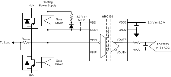 Figure 1 AMC1301
Functional Block Diagram
Figure 1 AMC1301
Functional Block DiagramEmbedded ADCs
Both the MSP430 and C2000 family of processors have embedded single-ended input ADCs so the question becomes: How do I get this differential signal into my single-ended data converter?
The simplest way to achieve this is to use only one output of the AMC1301 leaving the second output floating. The down side to this design is that only half the output voltage swing is available to the data converter, reducing the dynamic range of the measurement. The analog input range to the AMC1301 is ±250 mV. With a fixed gain of 8.2, the VOUTN and VOUTP voltages are ±1.025 V centered around the 1.44-V common-mode output as shown in Figure 2. Differentially, the output voltage is ±2.05 V.
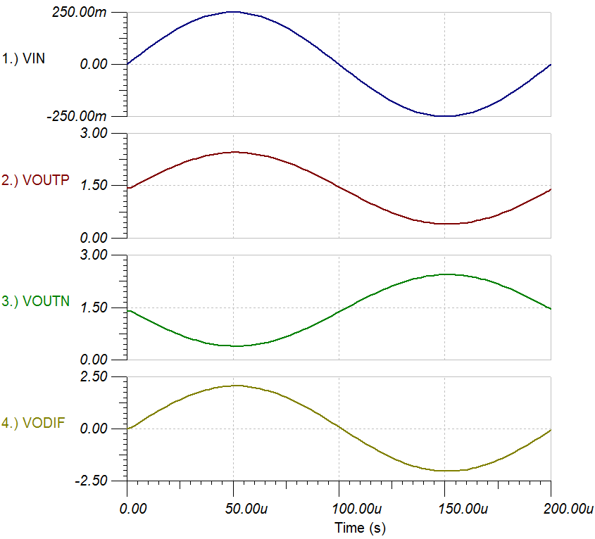 Figure 2 Differential Output Voltage
The addition of a differential to single-ended amplifier output stage, shown in Figure 3, allows the full output range of the AMC1301 to be provided to the ADC.
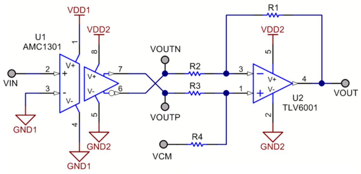 Figure 3 Differential to Single-Ended Output
Assuming a full scale sine wave of ±250 mV is applied at VIN; the internal gain of the AMC1301 provides 2.05 Vpk-pk outputs at points VOUTP and VOUTN which are 180° out of phase. The difference between these signals, VODIF, is 4.1 Vpk-pk. When R1 = R4 and R2 = R3, Equation 1 shows the transfer function of the output stage.
With equal value resistors for R1 through R4 in Equation 1 and VCM set to 2.5 V,Equation 2 reduces to:
The plots of Figure 4 show the input voltage and output voltages of the AMC1301 along with the output voltage of the final differential to single-ended output stage. Note that the differential voltage of ±2.05 V is transposed to a single-ended signal from 0.5 to 4.5 V.
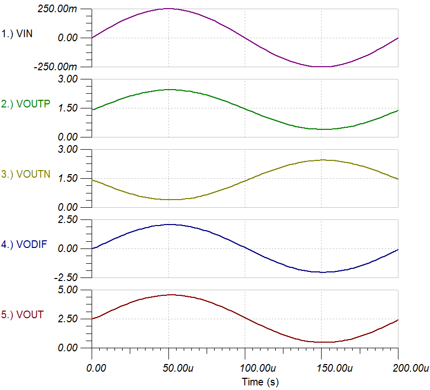 Figure 4 Single-Ended Output Voltage
Depending on the input voltage range of the ADC, gain or attenuation can be incorporated into the differential to single-ended stage to adjust the output swing. The output common-mode voltage can be adjusted to fit the input needs of the ADC as well.
Design Example
The ADC12 found on the MSP430 devices have an input voltage range of 0–2.5 V when using the internal voltage reference. Using the VOUTP from the AMC1301 can provide the ADC12 with an input signal ranging from 0.415 V to 2.465 V, well within the input range of the converter while only using half the input range of the AMC1301. As Figure 5 shows, using a differential to single-ended amplifier configuration with a gain of 0.5 and common mode voltage of 1.25 V, the entire voltage range of the AMC1301 can be applied to the ADC12.
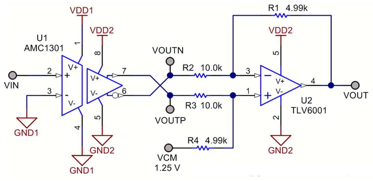 Figure 5 Scaled
Differential to Single-Ended Output
Figure 5 Scaled
Differential to Single-Ended OutputAlternative Device Recommendations
The AMC1100 or AMC1200 provide basic isolation with similar performance to the AMC1301 at a lower price point. Forthe TLV170 provides this option for applications that require a bipolar output.
| Device | Optimized Parameter | Performance Trade-Off |
|---|---|---|
| AMC1100 | Galvanic Isolation up to 4250 VPEAK | Lower Transient Immunity |
| AMC1200 | Galvanic Isolation up to 4250 VPEAK | Basic Isolation versus Reinforced |
| TLV170 | Bi-polar operation to ±18 V | Higher input bias current |
Conclusion
While it is possible to use a single output of the AMC1301 to drive a single-ended ADC, adding a differential to single-ended op-amp stage at the output ensures the target application has the largest possible dynamic range.