SBAA534 March 2022 ADC128S102-SEP , ADC128S102QML-SP , ADS1278-SP , ADS1282-SP , LF411QML-SP , LM101AQML-SP , LM111QML-SP , LM119QML-SP , LM124-SP , LM124AQML-SP , LM136A-2.5QML-SP , LM139-SP , LM139AQML-SP , LM148JAN-SP , LM158QML-SP , LM185-1.2QML-SP , LM185-2.5QML-SP , LM193QML-SP , LM4050QML-SP , LM6172QML-SP , LM7171QML-SP , LMH5401-SP , LMH5485-SEP , LMH5485-SP , LMH6628QML-SP , LMH6702QML-SP , LMH6715QML-SP , LMP2012QML-SP , LMP7704-SP , OPA4277-SP , OPA4H014-SEP , OPA4H199-SEP , THS4304-SP , THS4511-SP , THS4513-SP , TL1431-DIE , TL1431-SP , TLC2201-SP , TLV1704-SEP
2.5 Settling Time
The final analysis verifies if the settling time at the ADC input is short enough. For each sampling, the ADC must charge its internal sample and hold capacitor. During the setup time, the charge is transferred over from the external buffer capacitor. After the setup time, the ADC driver must be strong enough to recharge the buffer capacitor on time.
The worst-case condition for the settling time is when the signal input is set to 10 V. This will generate the max Vdiff output of –2.5 V or –2.499541 V, to be precise. Figure 2-13 illustrates using the DC Analysis option in the TINA-TI simulator to find the exact voltage that the 10-V input voltage generates at the ADC input.
 Figure 2-13 Use DC Analysis ➜ Calculate
Nodal Voltages Option to Identify the Precise Input Voltage to the ADC
Figure 2-13 Use DC Analysis ➜ Calculate
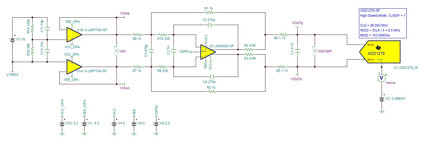
Nodal Voltages Option to Identify the Precise Input Voltage to the ADCThe ADS1278 simulation model provides the output of the sample-and-hold capacitor. If the voltage settles correctly it is exactly at –2.499541 V. Figure 2-14 shows this voltage is applied to this pin in the simulation via an extra voltage source, plus a voltage meter to measure the error from that expected voltage.
 Figure 2-14 Complete AFE System for
Settling Time Analysis
Figure 2-14 Complete AFE System for
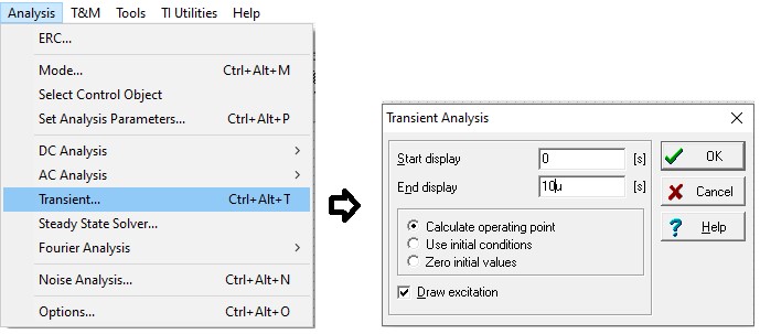
Settling Time AnalysisFigure 2-15 illustrates how the simulation is activated by selecting the TC transfer option from the analysis window.
 Figure 2-15 Select TC Transfer Option to
Analyze the Settling Time
Figure 2-15 Select TC Transfer Option to
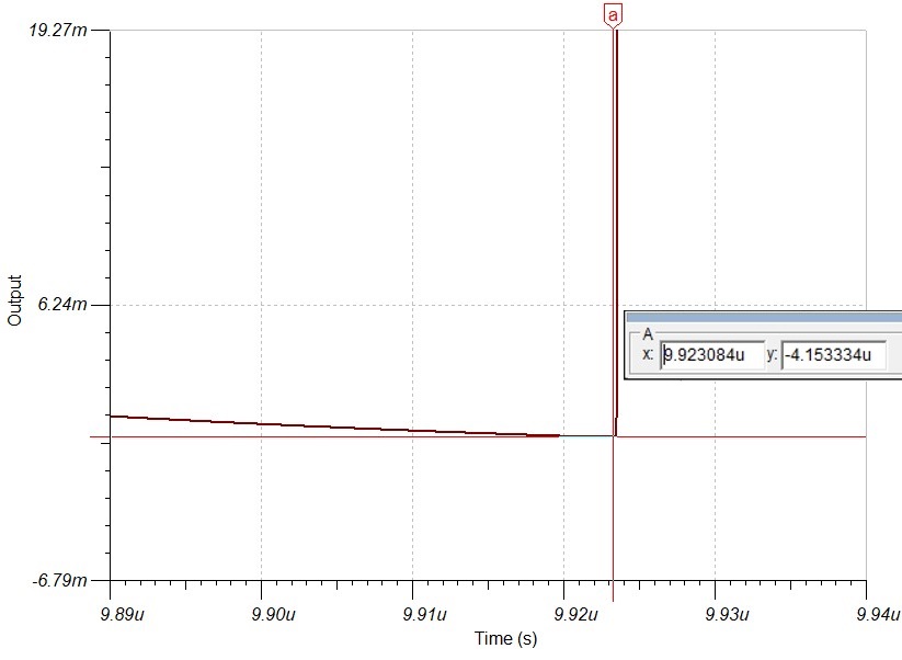
Analyze the Settling TimeFigure 2-16 shows a zoomed in view of the graph of the error voltage after the settling of –4.153 μV. This error appears as a gain error, and reduces to approximately 0 V at 0-V input. In relation to the full excitation of –2.5 V, these –4.153 μV translate into a gain error of 0.0001663% or –1.663 ppm. This represents roughly a 20-bit resolution, hence the settling error is small enough to meet the original design goal of > 16 ENOB.
 Figure 2-16 Simulation Result of the
Sample-and-Hold Capacitor Voltage Error of the ADS1278 at the End of the
Settling Window
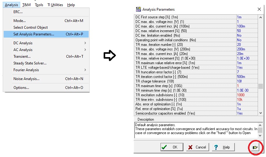
 Figure 2-17 Adjusting Analysis Parameters
for High Resolution (Numbers in Red), Press On the ‘Hand Icon’ to Get the Full
List