SBOA443 March 2021 INA293
4 Output Filter Discussion and Design
With the above approximations, we now have a range of values for potential resistances, RFILT, and capacitances, CFILT, that can be used to design the charge bucket filter for a given acquisition time. The challenge now set is the design of a filter that allows convergence to 1/2LSB, but also maintains system stability. With this information, we can design a filter that optimizes to this criterion by examining the output impedance of the amplifier in question, and how that amplifier will interact with the attached filter to drive the sampling node.
Here, we will examine the design of the INA293 with the ADS8860, a 16-bit, 1MSPS true differential input device. This device was chosen to examine potential maximization of sampling rate for the INA293, as lower resolution, or lower acquisition time would result in relaxed design constraints here.
Using the ADS8860 data sheet, we can determine the following parameters as shown in ADS8860 Key Specifications.
| Parameter | Value |
|---|---|
| ADS8860 Resolution | 16 bits |
| ADS8860 Conversion Time (maximum) | 710 ns |
| ADS8860 Acquisition Time (minimum) | 290 ns |
| Sample and Hold Capacitance, CSH | 59 pF |
Beginning with these values, and using the expressions derived in the previous section, the following calculated values are shown in Analog Engineer's Calculator Results.
| Parameter | Value |
|---|---|
| 1/2 LSB, FSR = 4.096V | 31.25 µV |
| CFILT, MIN = 10*CSH | 590 pF ≅ 600 pF |
| CFILT, NOM = 20*CSH | 1180 pF ≅ 1200 pF |
| CFILT, MAX = 30*CSH | 1770 pF ≅ 1800 pF |
τC, min | 35.93 ns |
τRC | 34.86 ns |
| RFILT, MIN | 7.4 Ω |
| RFILT, NOM | 29.55 Ω |
| RFILT, MAX | 59.1 Ω |
Bandwidth Required, Nominal | 18.3 Mhz |
Examining the calculated values, it can immediately be observed that the required estimated bandwidth is much larger than the 1.2MHz offered by the INA293, and therefore, this ADC is most likely not able to be correctly driven at its 1MSPS default sampling rate by the INA293. Therefore, the sampling rate will need to be relaxed. However, this paper will continue to examine this design flow to provide context to the reader as to the behavior such a design will exhibit prior to correcting this, as iteration in a design such as this is key in optimizing the design for the given application.
Using the techniques discussed in Closed-Loop Analysis of Load-Induced Amplifier Stability Issues Using ZOUT, a good starting place is to examine the output impedance of the INA293. Examining the INA293 spice model, it can be confirmed Using a small signal input placed at the output of the device that the model contains model parameters for the output impedance of the device, and can therefore be used to perform simulations, such as examining device stability, and examining the amplifier's ability to properly drive the ADC sample and hold circuitry. An example of this circuit and its corresponding output are shown in INA293 ZOUT Test Circuit and INA293 ZOUT Output Impedance below.
 Figure 4-1 INA293 ZOUT Test Circuit
 Figure 4-2 INA293 ZOUT Output Impedance
Next, examining the presence of a non-isolated capacitive load on this output for each of the filter capacitance options renders the following output for each of these loads as shown in ZEQ for Various CFILT.
 Figure 4-3 ZEQ for Various CFILT
The presence of these capacitors create a set of complex conjugate poles with the output impedance of the amplifier, and therefore steps need to be taken to ensure that the amplifier will remain stable over the range of frequencies.
Examining the regions where the INA293 output impedance and each capacitor close on one another, it can be seen that the output of the INA293 corresponds with a roughly singly inductive curve, due to the 20dB per decade increase of the impedance over frequency (note that the above figure exhibits impedance in ohms on the y-axis, not in dB). This system can be therefore be approximated as a second order pole approximation, where the poles of the system are given as:
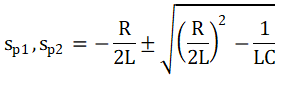
For the value of these poles to be real, the second term of this equation must result in a positive value. Taking this term and solving the inequality of this expression, it can be shown that
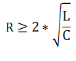
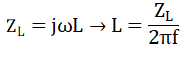
Or a resistance must be present that is greater than the interaction of the inductive portion of the curve with the added CFILT load. The inductive portion of the curve can be approximated at each point by the traditional formula for inductance over frequency, or
Approximating this inductance for each point on the curve, a resistor value for each case is calculated in Minimum RFILT Approximations for Stability.
| CFILT (pF) | Crossing Frequency (MHz) | ZL, approx. (Ω) | L, approx. (µH) | RFILT, Calculated (Ω) |
|---|---|---|---|---|
600 | 4.5 | 55 | 1.95 | 114 |
1200 | 3 | 45 | 2.39 | 89 |
1800 | 2.5 | 40 | 2.55 | 75 |
This provides a general starting point for RFILT, although this value may need to be adjusted based on ADC topology or settling.