SBOA444 November   2020 TMCS1100


  1.   Trademarks
  2. 1Introduction
  3. 2Implementation Block Diagram
  4. 3Hardware Implemenation
    1. 3.1 Analog Inputs
      1. 3.1.1 Voltage Measurement Analog Front End
      2. 3.1.2 Current Measurement Analog Front End
    2. 3.2 MSP432 LaunchPad Connections
    3. 3.3 PCB Layout Recommendations
  5. 4How to Implement Software for Metrology Testing
    1. 4.1 Setup
      1. 4.1.1 Clock
      2. 4.1.2 UART Setup for GUI Communication
      3. 4.1.3 Real-Time Clock (RTC)
      4. 4.1.4 Direct Memory Access (DMA)
      5. 4.1.5 ADC Setup
    2. 4.2 Foreground Process
      1. 4.2.1 Formulas
        1. 4.2.1.1 Standard Metrology Parameters
        2. 4.2.1.2 Power Quality Formulas
    3. 4.3 Background Process
      1. 4.3.1 per_sample_dsp( )
        1. 4.3.1.1 Voltage and Current ADC Samples
        2. 4.3.1.2 Pure Waveform Samples
        3. 4.3.1.3 Frequency Measurement and Cycle Tracking
      2. 4.3.2 LED Pulse Generation
      3. 4.3.3 Phase Compensation
  6. 5Metrology Accuracy Testing
    1. 5.1 Test Setup
    2. 5.2 Results
  7. 6Schematics
  8. 7References

Implementation Block Diagram

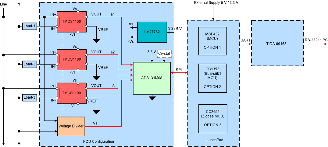
The Block Diagram depicts the block diagram of the example TMCS1100 PDU implementation tested in this application note. This implementation uses the TMCS1100 Hall-effect current sensor, ADS131M08 delta-sigma ADC, the LM27762 charge pump, a metrology microcontroller, and an isolated UART to RS-232 board.

GUID-20201005-CA0I-2GHV-5BTP-VH8JCW7F0P2F-low.gif Figure 2-1 Block Diagram.
In this implementation, there are four ADC channels that are used. One of these channels senses the inlet voltage. For sensing the voltage, a voltage divider divides the Mains voltage to a range that can be sensed by an ADC. The choice of voltage divider resistors for the voltage channel is selected to ensure the mains voltage is divided down to adhere to the normal input ranges of the ADS131M08 device. Since the ADS131M08 ADCs have a large dynamic range and a large dynamic range is not needed to measure voltage, the voltage front-end circuitry is purposely selected so that the maximum voltage seen at the inputs of the voltage channel ADCs are only a fraction of the full-scale voltage. By reducing the voltage fed to the ADS131M08 voltage ADC, voltage-to-current crosstalk, which actually affects metrology accuracy more than voltage ADC accuracy, is reduced at the cost of voltage accuracy, thereby resulting in more accurate energy measurements at lower currents.

The other three channels of this device are used to sense the current of the different outlets. Each current channel uses the TMCS1100 Hall-effect current sensor to translate the sensed current into a voltage sensable by the ADS131M08 ADC. To fit within the input voltage range of the ADS131M08, level shifting is necessary. This level shifting is accomplished by using the LM27762 charge pump to create 2.5-V and –2.5-V voltage rails that power the TMCS1100.

The ADS131M08 uses a crystal connected to its XTAL1 and XTAL2 pins to generate an internal clock, fCLKIN. The ADS131M08 internally divides this clock by two and uses this divided down clock as the delta-sigma modulation clock, fM. The sampling rate of the ADS131M08 is therefore defined as
fs = fM / OSR = fCLKIN / (2 × OSR). Whenever there are new samples available, the ADS131M08 asserts its DRDY pin to notify the microcontroller that new samples are available. The microcontroller would then use one of its SPI interfaces and its DMA to get the voltage and current samples from the ADS131M08 device. The microcontroller uses the new voltage and current samples for the calculation of the metrology parameters, such as the power and RMS readings.

The ADC connections to the microcontroller are brought out the LaunchPad connector of the design, which allows for different microcontrollers to be used as the metrology microcontroller by connecting the corresponding microcontroller LaunchPad to the LaunchPad connector of the design. For this specific implementation, the MSP432P4111 device was used as the metrology microcontroller by connecting the MSP-EXP432P4111 LaunchPad to the LaunchPad connector of the design.

For calibrating and testing the design, a PC GUI was used. The PC GUI communicates to the design through an isolated RS-232 connection created by the TIDA-00163 board. The TIDA-00163 board connects to a set of UART transmit (pin P2.5 on the MSP432) and receive (pin P2.3 on the MSP432) pins pin from the MSP432. The board isolates the signals from these pins and then translates the isolated signal to RS-232 signal levels. The resulting RS-232 signals are sent to the RS-232 connector of the TIDA-00163, which the PC is connected to.