SBOA562 april 2023 INA240
4 Near-Zero Vsense Operating Mode in Some Legacy CSA
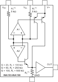
The INA193-INA198 devices use a unique circuit topology that provides common-mode range extending from −16 V to 80 V while operating from a single power supply. As shown in Figure 4-1, when the common-mode voltage is positive, amplifier A2 is active. The differential input voltage, (VIN+) − (VIN-) applied across RS, is converted to a current through a resistor. This current is converted back to a voltage through RL, and then amplified by the output buffer amplifier. When the common-mode voltage is negative, amplifier A1 is active. The differential input voltage, (VIN+) − (VIN-) applied across RS, is converted to a current through a resistor. This current is sourced from a precision current mirror whose output is directed into RL converting the signal back into a voltage and amplified by the output buffer amplifier.
 Figure 4-1 INA193-INA198 Block Diagram
At near-zero Vsense, the output current is very low, the collector-base (or Emitter-base) leakage of the output transistor becomes prominent and can effectively shut down the transistors driving the output transistor. Consequently, the output cannot continue to swing toward ground in proportion to the decreasing input voltage. The lowest output level appears as a floor that is higher than the expected output voltage. This is the reason why 20 mV and below is considered low Vsense for this family of devices, where the output deviation becomes noticeable.
Another factor affecting output accuracy is common mode voltage, Vcm. Normally one of the two amplifiers, A1 or A2, is active and dominates. However, when common mode input voltage is between ground and supply voltage, both A1 and A2 can be active but neither is dominating. The deviation from linear operation becomes greatest the closer Vsense approaches zero, making this region the least accurate.
INA200 through INA208 are a family of nine devices based on the INA193-INA198. Comparators and references are included to these devices, which makes overcurrent protection (OCP) convenient. Because the analog core remains the same, take care when operating these devices with near-zero Vsense. Similar to the INA193-INA198, the least accurate region of operation is when Vcm is between ground and supply voltage.