SFFS006B November 2020 – March 2024 LMR33610 , LMR33620 , LMR33630 , LMR33640
4.2 HSOIC Package
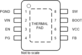
Figure 4-2 shows the LMR336x0 pin diagram for the HSOIC package. For a detailed description of the device pins please refer to the Pin Configuration and Functions section in the appropriate device data sheet.
 Figure 4-2 Pin
Diagram
Figure 4-2 Pin
DiagramTable 4-6 Pin FMA for Device Pins
Short-Circuited to Ground
| Pin Name | Pin No. | Description of Potential Failure Effect(s) | Failure Effect Class |
|---|---|---|---|
| PGND | 1 | No effect | D |
| VIN | 2 | Device will not operate. No output voltage will be generated. Output capacitors will discharge through input short. Large reverse current may damage device. | A |
| N/C | 3 | Loss of ENABLE functionality Device will remain in shutdown mode. | B |
| BOOT | 4 | Power good functionality will be lost. | B |
| VCC | 5 | The regulator will operate at maximum duty cycle. Output voltage will rise to approximately the input voltage (VIN) level. Possible damage to customer load and output stage components may occur. No effect on device. | B |
| AGND | 6 | No effect | D |
| FB | 7 | Damage to internal circuits | A |
| PG | 8 | Damage to internal power FETs and other internal circuits | A |
Table 4-7 Pin FMA for Device Pins Open-Circuited
| Pin Name | Pin No. | Description of Potential Failure Effect(s) | Failure Effect Class |
|---|---|---|---|
| PGND | 1 | Possible device damage. | A |
| VIN | 2 | Loss of output voltage. | B |
| EN | 3 | Loss of ENABLE functionality. Erratic operation; probable loss of regulation. | B |
| PG | 4 | PG functionality will be lost. | B |
| FB | 5 | Loss of output voltage regulation. Output voltage may rise or fall outside of intended regulation window. | B |
| VCC | 6 | VCC LDO will be unstable. Loss of output voltage regulation and possible damage to internal circuits. | A |
| BOOT | 7 | Loss of output voltage regulation; low or no output voltage. | B |
| SW | 8 | Loss of output voltage. | B |
Table 4-8 Pin FMA for Device Pins
Short-Circuited to Adjacent Pin
| Pin Name | Pin No. | Shorted to | Description of Potential Failure Effect(s) | Failure Effect Class |
|---|---|---|---|---|
| PGND | 1 | VIN | Device will not operate. No output voltage will be generated. Output capacitors will discharge through input short. Large reverse current may damage device. | A |
| VIN | 2 | EN | This is a valid connection for the EN input. Enable functionality will be lost; the device will remain on. | B |
| EN | 3 | PG | Erratic operation; probable loss of regulation. | B |
| FB | 5 | VCC | Output voltage will drop to near zero volts. | B |
| VCC | 6 | BOOT | Loss of output regulation, possible damage to internal circuits | A |
| BOOT | 7 | SW | Damage to internal circuits. No output voltage will be produced. | A |
Table 4-9 Pin FMA for Device Pins
Short-Circuited to VIN
| Pin Name | Pin No. | Description of Potential Failure Effect(s) | Failure Effect Class |
|---|---|---|---|
| PGND | 1 | Device will not operate. No output voltage will be generated. Output capacitors will discharge through input short. Large reverse current may damage device. | A |
| VIN | 2 | No effect. | D |
| EN | 3 | No damage to device. Loss of ENABLE functionality. | B |
| PG | 4 | Damage to internal circuits. | A |
| FB | 5 | Damage to internal circuits will occur for VIN > 5.5V. | A |
| VCC | 6 | Damage to internal circuits for VIN > 5.5V. | A |
| BOOT | 7 | Damage to internal circuits | A |
| SW | 8 | The output voltage will rise to approximately the level of VIN. Customer load will be damaged. Possible damage to device. | A |