SFFS308 October 2021 TPS62402-Q1
1 Pin Failure Mode Analysis (Pin FMA)
This section provides a failure mode analysis (FMA) for the pins of the TPS62402-Q1. The failure modes covered in this document include the typical pin-by-pin failure scenarios:
- Pin short-circuited to ground (see Table 1-2)
- Pin open-circuited (see Table 1-3)
- Pin short-circuited to an adjacent pin (see Table 1-4)
- Pin short-circuited to supply (see Table 1-5)
Table 1-2 through Table 1-5 also indicate how these pin conditions can affect the device as per the failure effects classification in Table 1-1.
| Class | Failure Effects |
|---|---|
| A | Potential device damage that affects functionality. |
| B | No device damage, but loss of functionality. |
| C | No device damage, but performance degradation. |
| D | No device damage, no impact to functionality or performance. |
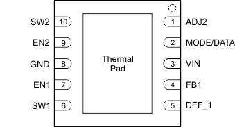
Figure 1-1 shows the TPS62402-Q1 pin diagram. For a detailed description of the device pins, see the Pin Configuration and Functions section in the TPS62402-Q1 data sheet.
 Figure 1-1 Pin Diagram
Following are the assumptions of use and the device configuration assumed for the pin FMA in this section:
- Assumption the device is running in the typical application, please refer to the 'Simplified Schematic' on the first page in the TPS62402-Q1 data sheet.
| Pin Name | Pin No. | Description of Potential Failure Effect(s) | Failure Effect Class |
|---|---|---|---|
|
ADJ2 |
1 |
Output voltage regulated to VIN (100% mode) |
B |
|
MODE/DATA |
2 |
Intended functionality |
D |
|
VIN |
3 |
Device does not power up, no output voltage |
B |
|
FB1 |
4 |
100% duty cycle mode, output voltage follows the input voltage |
B |
|
DEF_1 |
5 |
Intended functionality |
D |
|
SW1 |
6 |
Potential device damage |
A |
|
EN1 |
7 |
Device is disabled, no output voltage |
B |
|
GND |
8 |
Normal operation |
D |
|
EN2 |
9 |
Device is disabled, no output voltage |
B |
|
SW2 |
10 |
Potential device damage |
A |
| Pin Name | Pin No. | Description of Potential Failure Effect(s) | Failure Effect Class |
|---|---|---|---|
|
ADJ2 |
1 |
Undetermined output voltage behavior; open loop operation |
B |
|
MODE/DATA |
2 |
Undetermined device operation |
B |
|
VIN |
3 |
Device does not power up, no output voltage |
B |
|
FB1 |
4 |
100% or 0% duty cycle operation, no regulated output voltage. Output voltage either follows the input voltage or no output voltage. |
B |
|
DEF_1 |
5 |
Undetermined output voltage behavior |
B |
|
SW1 |
6 |
Device not functional, open loop operation |
B |
|
EN1 |
7 |
Device is either enabled or disabled. If enabled, output voltage is regulated to its nominal value. If disabled, no output voltage |
B |
|
GND |
8 |
Device does not power up, no output voltage |
B |
|
EN2 |
9 |
Device is either enabled or disabled. If enabled, output voltage is regulated to its nominal value. If disabled, no output voltage |
B |
|
SW2 |
10 |
Device not functional, open loop operation |
B |
| Pin Name | Pin No. | Shorted to | Description of Potential Failure Effect(s) | Failure Effect Class |
|---|---|---|---|---|
|
ADJ2 |
1 |
2 |
Potential device damage |
A |
|
FB1 |
4 |
5 |
Wrong output voltage regulated |
C |
|
Sw1 |
6 |
7 |
Potential device damage |
A |
|
EN2 |
9 |
10 |
Potential device damage |
A |
| Pin Name | Pin No. | Description of Potential Failure Effect(s) | Failure Effect Class |
|---|---|---|---|
|
ADJ2 |
1 |
Potential device damage |
A |
|
MODE/DATA |
2 |
Normal operation |
D |
|
VIN |
3 |
Normal operation |
D |
|
FB1 |
4 |
Potential device damage |
A |
|
DEF_1 |
5 |
Normal operation |
D |
|
SW1 |
6 |
Potential device damage |
A |
|
EN1 |
7 |
Normal operation |
D |
|
GND |
8 |
Device does not power up, no output voltage |
B |
|
EN2 |
9 |
Normal operation |
D |
|
SW2 |
10 |
Potential device damage |
A |