SLAA988A December 2020 – January 2022 TAS2563
1.9 Sense Pins
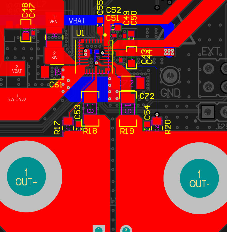
VSNS_N and VSNS_P are the voltage sense negative and positive inputs, respectively. These inputs are connected to the Class-D outputs (VSNS_N to OUT_N and VSNS_P to OUT_P) after the ferrite bead filter.
When routing these pins to the ferrite bead filter, it is necessary to the make the connection to its respective output at the speaker terminal, not to a pin or trace. In addition, TI recommends adding a 1-kΩ resistor for each voltage sense path. This practice helps to reduce emissions and reduce ICN increments that result from the EMI filter.
 Figure 1-11 VSNS_P and VSNS_N Connections