SLAU776A May 2018 – December 2023 ADC12DL2500 , ADC12DL3200
- 1
- Abstract
- Trademarks
- 1Introduction
- 2Equipment
-
3Setup Procedure
- 3.1 Install the High Speed Data Converter (HSDC) Pro Software
- 3.2 Install the Configuration GUI Software
- 3.3 Connect the EVM and TSW14DL3200EVM
- 3.4 Connect the Power Supplies to the Boards (Power Off)
- 3.5 Connect the Signal Generators to the EVM (*RF Outputs Disabled Until Directed)
- 3.6 Turn On the TSW14DL3200EVM Power and Connect to the PC
- 3.7 Turn On the ADC12DLXX00EVM 5-V Power Supply and Connect to the PC
- 3.8 Turn On the Signal Generator RF Outputs
- 3.9 Open the ADC12DLXX00EVM GUI and Program the ADC and Clocks
- 3.10 Calibrate the ADC Device on the EVM
- 3.11 Open the HSDC Software and Load the FPGA Image to the TSW14DL3200EVM
- 3.12 Capture Data Using the HSDC Pro Software
- 4Device Configuration
- A Troubleshooting the ADC12DL3200EVM
- B Optional ADC12DL3200EVM Configurations
- C Revision History
1 Introduction
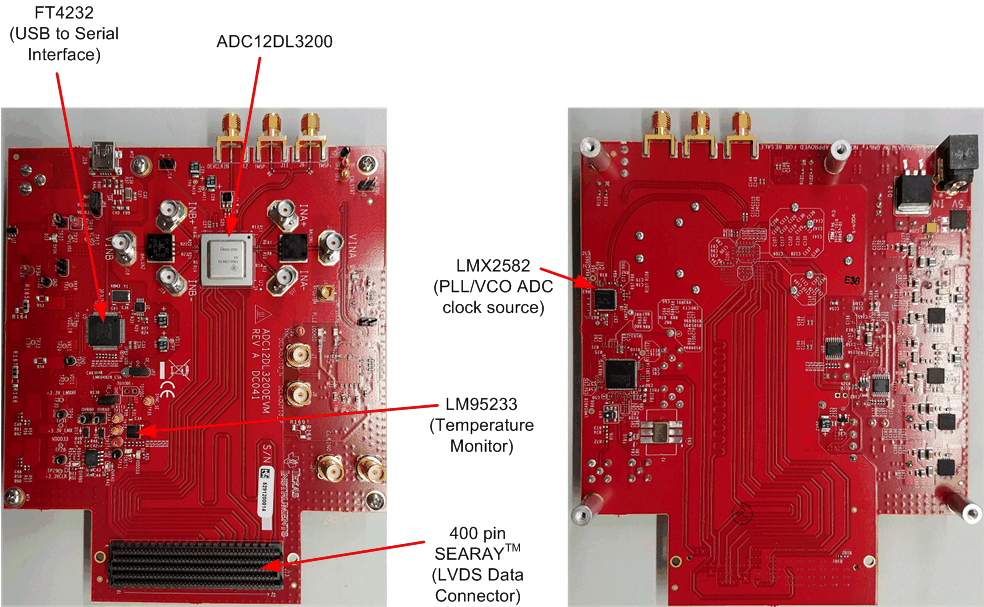
The ADC12DLXX00 is a dual-channel, 12-bit ADC, capable of operating at sampling rates up to 3.2 Giga-samples per second (GSPS) and 2.5 GSPS in dual-channel mode, or 6.4 GSPS and 5 GSPS in single-channel mode. The ADC12DLXX00EVM device output data is transmitted over a high-speed LVDS interface. This evaluation board also includes the following important features:
- Transformer-coupled signal input network allowing a single-ended signal source from 500 kHz to 9 GHz
- The LMX2582 clock synthesizer generates the ADC sampling clock
- Transformer-coupled clock input network to test the ADC performance with an external low-noise clock source
- LM95233 temperature sensor
- Device register programming through USB connector and FTDI USB-to-SPI bus translator
- High-speed LVDS data output over a
400-pin SEARAY® interface
connector Note:
While this is the same connector used for FMC standard boards, the LVDS data, clock and strobe pinout is proprietary to the ADC12DL3200EVM, TSW14DL3200EVM, and other compatible boards.
The digital data from the ADC12DLXX00EVM board is quickly and easily captured with the TSW14DL3200EVM data capture board.
The TSW14DL3200EVM supports 48 data pairs (Demux = 1) up to 1600 Mbps.
The TSW14DL3200EVM captures the LVDS data, decodes the data, stores the data in memory, and then uploads the data to a connected PC through a USB interface for analysis. The High-Speed Data Converter Pro (HSDC Pro) software on the PC communicates with the hardware and processes the data.
In the following sections of this document, the ADC12DLXX00EVM is referred to as the EVM and the ADC12DLXX00 device is referred to as the ADC device.