SLLA500 December 2020 TUSB2E22
5 PCB Stackup for eUSB2 Applications
Since eUSB2 supports the same maximum signaling speed as USB 2.0 at 480 Mbps, the PCB stackup requirements are similar. To maintain signal integrity and reduce EMI, a 4-layer PCB or greater is recommended. FR4 is a suitable and affordable material for both eUSB2 and USB 2.0 PCBs with low insertion loss at the Nyquist frequency of 240 MHz of less than 0.1 dB per inch.
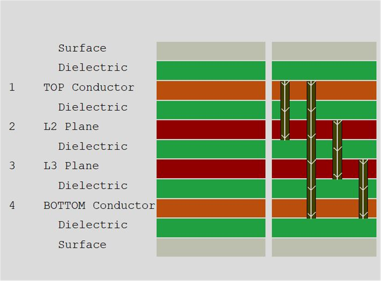
Figure 5-1 shows an example PCB stackup with trace routing on layer 1, ground on layer 2, power on layer 3 and trace routing on layer 4. This stack-up assumes eUSB2 and USB differential microstrip routing on the outer layers.
 Figure 5-1 Sample 4-Layer PCB
Stackup
Figure 5-1 Sample 4-Layer PCB
StackupReferencing the channel specifications from Table 7-6 in the eUSB2 Physical Layer Supplement, duplicated in Table 5-1, FR4 is adequate for most eUSB2 applications.
| Parameter | Max | Units |
|---|---|---|
| Host-to-repeater insertion loss(1) (2) | –1.2 | dB |
| Repeater-to-connector insertion loss | –2 | dB |