SLLA502A October 2020 – December 2021 TCAN1042-Q1 , TCAN1042G-Q1 , TCAN1042GV-Q1 , TCAN1042H-Q1 , TCAN1042HG-Q1 , TCAN1042HGV-Q1 , TCAN1042HV-Q1 , TCAN1042V-Q1
1 Overview
This document contains information for TCAN1042-Q1 and TCAN1042V-Q1 (as well as the TCAN1042H-Q1, TCAN1042G-Q1, TCAN1042HV-Q1, TCAN1042GV-Q1, TCAN1042HG-Q1 and TCAN1042HGV-Q1). These are Controller Area Network (CAN) transceivers in the SOIC (D) and VSON (DRB) packages to aid in a functional safety system design. Information provided are:
- Functional Safety Failure In Time (FIT) rates of the semiconductor component estimated by the application of industry reliability standards
- Component failure modes and their distribution (FMD) based on the primary function of the device
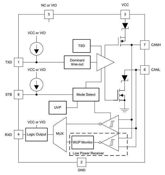
- Pin Failure Mode Analysis (FMA) for the device pins of TCAN1042-Q1 and TCAN1042V-Q1Figure 1-1 shows the device functional block diagram for reference. TCAN1042V-Q1 has the VIO input at pin 5, while TCAN1042-Q1 has a no connect (NC) at pin 5.
 Figure 1-1 TCAN1042-Q1/TCAN1042V-Q1 Functional Block Diagram
TCAN1042-Q1 and TCAN1042V-Q1 were developed using a quality-managed development process, but was not developed in accordance with the IEC 61508 or ISO 26262 standards.