SLLA519 November 2020 ISO1540-Q1 , ISO1541-Q1
4.1 ISO1541-Q1 in 8-D Package
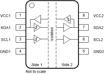
Figure 4-1 shows the ISO1541-Q1 pin diagram for the 8-D package. For a detailed description of the device pins please refer to the Pin Configuration and Functions section in the ISO154x-Q1 data sheet.
 Figure 4-1 Pin Diagram (8-D)
Package
Figure 4-1 Pin Diagram (8-D)
PackageTable 4-2 Pin FMA for Device Pins
Short-Circuited to Ground
| Pin Name | Pin No. | Description of Potential Failure Effect(s) | Failure Effect Class |
|---|---|---|---|
| VCC1 | 1 | No power to the device on side-1. Observe that the absolute maximum ratings for SDA1/SCL1 are met; otherwise device damage may be plausible. | A |
| SDA1 | 2 | SDA1 stuck to low, makes SDA2 also low. Communication corrupted to and from the master node. | B |
| SCL1 | 3 | SCL1 stuck to low, makes SCL2 also low. Communication corrupted to and from the master. | B |
| GND1 | 4 | Device continues to function as expected. Normal operation. | D |
| GND2 | 5 | Device continues to function as expected. Normal operation. | D |
| SCL2 | 6 | SCL2 stuck low. Data communication from master SCL1 to slave SCL2 lost. Communication corrupted. | B |
| SDA2 | 7 | SDA2 stuck low, makes SDA1 also low. Communication corrupted to and from the master node. | B |
| VCC2 | 8 | No power to the device on side-2. Observe that the absolute maximum ratings for SDA2/SCL2 are met; otherwise device damage may be plausible. | A |
Table 4-3 Pin FMA for Device Pins
Open-Circuited
| Pin Name | Pin No. | Description of Potential Failure Effect(s) | Failure Effect Class |
|---|---|---|---|
| VCC1 | 1 | Operation undetermined. Either device is unpowered and SDA2/SCL2 are pulled to logic high to external pull-up resistors or through internal ESD diode on SDA1/SCL1 pin, device can power up if SDA1/SCL1 are logic high. If abs max rating of SDA1/SCL1 is not observed, device damage plausible. | A |
| SDA1 | 2 | No data communication to and from the master node possible. | B |
| SCL1 | 3 | Clock missing, so no I2C communication possible. | B |
| GND1 | 4 | Device unpowered on side1. SDA2/SCL2 are logic high via external pull-up resistors. | B |
| GND2 | 5 | Device unpowered on side2. SDA1/SCL1 are logic high via external pull-up resistors. | B |
| SCL2 | 6 | Clock missing, so no I2C communication possible. | B |
| SDA2 | 7 | No data communication possible. | B |
| VCC2 | 8 | Operation undetermined. Either device is unpowered and SDA1/SCL1 are pulled to logic high to external pull-up resistors or through internal ESD diode on SDA2/SCL2 pin, device can power up if SDA2/SCL2 are logic high. If abs max rating of SDA2/SCL2 is not observed, device damage plausible. | A |
Table 4-4 Pin FMA for Device Pins
Short-Circuited to Adjacent Pin
| Pin Name | Pin No. | Shorted to | Description of Potential Failure Effect(s) | Failure Effect Class |
|---|---|---|---|---|
| VCC1 | 1 | SDA1 | SDA1 stuck high. Communication corrupted. If SDA2 is driven logic low for extended duration, SDA1 stuck high creates short between supply and ground, possible device damage. | A |
| SDA1 | 2 | SCL1 | I2C Communication corrupted. | B |
| SCL1 | 3 | GND1 | SCL1 stuck to low, makes SCL2 also low. Communication corrupted to and from the master. | B |
| GND1 | 4 | SCL1 | Already considered in above row. | B |
| GND2 | 5 | SCL2 | SCL2 stuck low. Data communication from master SCL1 to slave SCL2 lost. Communication corrupted. | B |
| SCL2 | 6 | SDA2 | I2C Communication corrupted. | B |
| SDA2 | 7 | VCC2 | SDA2 stuck high. Communication corrupted. If SDA1 is driven logic low for extended duration, SDA2 stuck high creates short between supply and ground, possible device damage. | A |
| VCC2 | 8 | SDA2 | Already considered in above row. | A |
Table 4-5 Pin FMA for Device Pins Short-Circuited to
supply
| Pin Name | Pin No. | Description of Potential Failure Effect(s) | Failure Effect Class |
|---|---|---|---|
| VCC1 | 1 | No effect. Normal operation. | D |
| SDA1 | 2 | SDA1 stuck high. Communication corrupted. If SDA2 is driven logic low for extended duration, SDA1 stuck high creates short between supply and ground, possible device damage. | A |
| SCL1 | 3 | SCL1 stuck high does not allow clock transitions to happen. I2C communication corrupted. | B |
| GND1 | 4 | Device side-1 unpowered. Observe that the absolute maximum ratings for SCL1/SDA1 pins of the device are met, otherwise device damage may be plausible. | A |
| GND2 | 5 | Device side-2 unpowered. Observe that the absolute maximum ratings for SCL2/SDA2 pins of the device are met, otherwise device damage may be plausible. | A |
| SCL2 | 6 | SCL2 stuck high. If SCL1 is driven low for extended duration, SCL2 stuck high creates a path for high current from supply to ground with possible device damage. | A |
| SDA2 | 7 | SDA2 stuck high. Communication corrupted. If SDA1 is driven logic low for extended duration, SDA2 stuck high creates short between supply and ground, possible device damage. | A |
| VCC2 | 8 | No effect. Normal operation. | D |