SLOA170B July 2012 – January 2021 DRV8242-Q1 , DRV8412 , DRV8424 , DRV8424E , DRV8425 , DRV8425E , DRV8426 , DRV8426E , DRV8428 , DRV8428E , DRV8434 , DRV8434E , DRV8436 , DRV8436E , DRV8701 , DRV8702-Q1 , DRV8702D-Q1 , DRV8703-Q1 , DRV8703D-Q1 , DRV8705-Q1 , DRV8706-Q1 , DRV8800 , DRV8801 , DRV8802 , DRV8802-Q1 , DRV8811 , DRV8812 , DRV8813 , DRV8814 , DRV8818 , DRV8821 , DRV8823 , DRV8823-Q1 , DRV8824 , DRV8824-Q1 , DRV8825 , DRV8828 , DRV8829 , DRV8832 , DRV8832-Q1 , DRV8833 , DRV8834 , DRV8840 , DRV8841 , DRV8842 , DRV8843 , DRV8844 , DRV8846 , DRV8848 , DRV8870 , DRV8874 , DRV8874-Q1 , DRV8876 , DRV8876-Q1 , DRV8880 , DRV8881 , DRV8885 , DRV8886 , DRV8889-Q1 , DRV8899-Q1 , DRV8935 , DRV8955
5 Changeable Holding Current Circuit
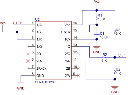
The circuit in Figure 5-1 can realize changeable holding current function by using the CD74HC123. The CD74HC123 is a dual, retriggerable, monostable multivibrator, with reset. In this application, the input STEP comes from the step signal of the motor driver ICs, such as DRV8818. The output VREF is applied to the VREF pin of the motor driver ICs to achieve changeable holding current.
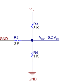
According to the principle of CD74HC123, when a pulse is applied to pin 1, there is a high output on pin 13, with a pulse width of 0.45 RX × CX starting at the falling edge of the signal on pin 1. When the signal frequency on pin 1 is bigger than 1 / (0.45 RX × CX), the high level on pin 13 maintains all the time. Figure 5-2 shows that by this time, the voltage on pin 13 stays high (Vcc), through a potential-divider network, an R4 × Vcc / (R4 + R2 // R3) output voltage is applied to the VREF pin of the motor driver IC.
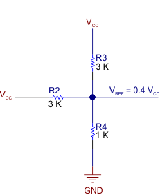
When the stepper motor is in holding state, there will be no pulse on the STEP, the level on pin 1 will be low so the output voltage on pin 13 will be driven low (GND), hence the VREF voltage becomes Vcc × (R2 // R4) / (R2 // R4 + R3), as shown in Figure 5-3. In this way, the holding current of the stepper motor can be set by choosing suitable resistors.
So the VREF can be automatically changed when the stepper motor enters into holding state. Note: to get a good performance of normal operation, adjust the value of RX and CX based on a target STEP signal to achieve a constant high level on pin 13 when the stepper motor is in normal operation. For example, if the frequency of the step signal is 1/15 Hz, that is, there are only four steps in one minute, then 1/15 > 1 / (0.45 RX × CX), so RX × CX must be larger than 33.3, so 10 M can be selected for RX, 10 µF can be selected for CX.
 Figure 5-1 Changeable Holding Current Circuit
 Figure 5-2 Output of Normal Operation
 Figure 5-3 Output of Holding State