SLUS696C June 2006 – February 2019 BQ26100
PRODUCTION DATA.
- 1 Features
- 2 Applications
- 3 Description
- 4 Revision History
- 5 Pin Configuration and Functions
- 6 Specifications
-
7 Detailed Description
- 7.1 Overview
- 7.2 Functional Block Diagram
- 7.3 Feature Description
- 7.4 Device Functional Modes
- 7.5
Programming
- 7.5.1 Communicating with the bq26100 Device
- 7.5.2 Memory Descriptions
- 7.5.3 SHA-1 Description
- 7.5.4 Key Programming Description
- 7.6 Register Maps
- 8 Application and Implementation
- 9 Power Supply Recommendations
- 10Layout
- 11Device and Documentation Support
- 12Mechanical, Packaging, and Orderable Information
7.5.1 Communicating with the bq26100 Device
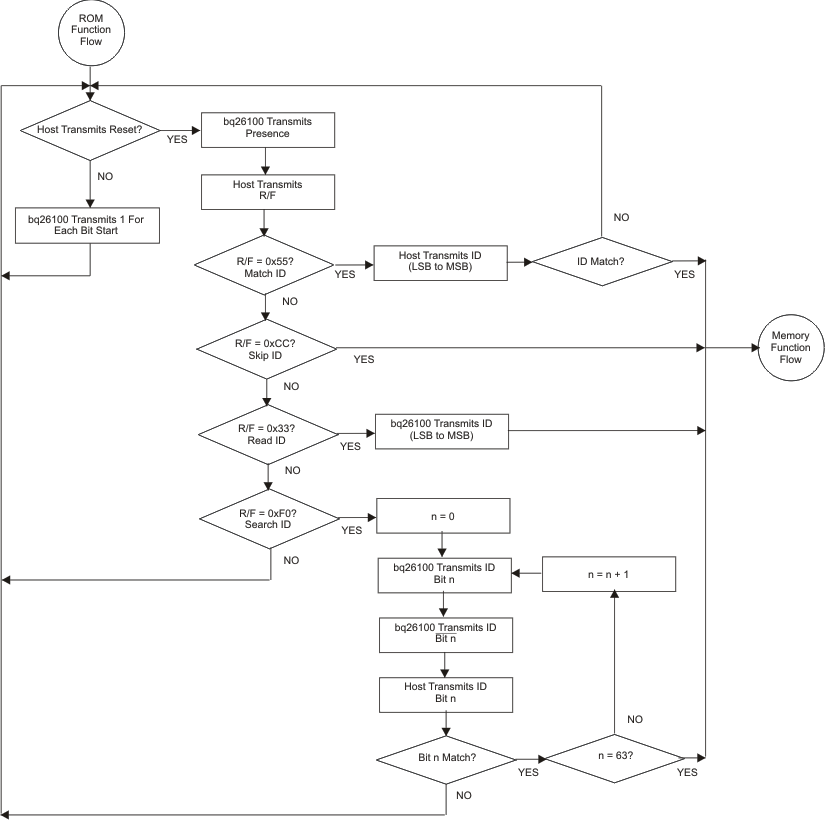
The bq26100 device communication protocol starts when the host pulls the bus low for reset time. All devices on the bus are to respond with a presence pulse, which is active low. The host can then transmit the ROM Function command, which is used to address the devices on the bus. The ROM functions include Match ID, Skip ID, Read ID, and Search ID.
| Match ID | The host transmits the 64-bit ID of the 1-wire based device to communicate. |
| Skip ID | No ID is necessary for communication. Used only if one device is connected to the host. |
| Read ID | The 1-wire slave transmits its 64 bit address. This command is only useful if there is only one device connected to the host. |
| Search ID | Useful if there are multiple devices on the bus. This command initiates a communication with a single device, but it is more useful in allowing the host to determine the address of every device on the bus. The Match ID can then be used to communicate with a specific addressed device. |
 Figure 8. ROM Function Flow Chart
 The 64-bit device ID is made up of an 8-bit family code, 48-bit random value, and a final 8-bit CRC (see Table 1).
Table 1. Format of 64-bit Device ID
| ID MSB | ID LSB | |
| CRC (8 bits) | Random Data (48 bits) | Family Code (8 bits, defaults to 0x09) |
Contact Texas Instruments if specific data should be programmed into the ID.
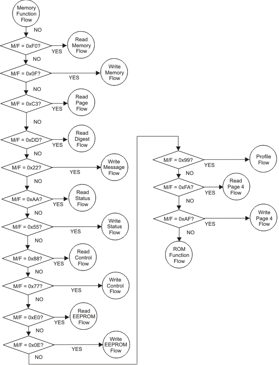
After the ROM function command is issued and the bq26100 device is selected, a Memory Function command can be issued. The Memory Function commands are Read Memory, Read EEPROM, Read Status, Read Page, Read Page 4, Read Digest, Read Control, Write Memory, Write Page 4, Write EEPROM, Write Status, Write Message, Write Control, and Profile.
Figure 9 shows the flow for the Memory Function selection. Figure 12 through Figure 15 illustrate the flow for each memory function.
 Figure 9. Memory Function Flow Chart
 The SDQ protocol requires a CRC calculation as part of the communication flow. The CRC, based on a polynomial of x8+x5+x4+1, is computed to determine data integrity and its use varies in the protocol. The Memory Function flows show what data are shifted through the CRC and when the value is transmitted from the slave. Each data byte used in the CRC calculation is pushed through the CRC shift register from LSB to MSB. The byte wide CRC computation is:
for (i = 0; i < 8; i++) {


   if (crc[0] ^ input[i])


     crc = (crc >> 1) ^ 0x8C;


   else


     crc = crc >> 1;


}
Where did the magic number 0x8C come from? CRC polynomials are defined such that the highest order simply shows the number of bits, so x8+x5+x4+1 defines an 8-bit value with a binary value of 00110001 (bits 0, 4, and 5 are 1 and all others are 0). Since the SDQ CRC is computed by shifting in the LSB, the polynomial must be used in reverse bit order – binary 10001100 or hexadecimal 0x8C.
The CRC value is reset to 0 prior to the first byte being shifted through. The CRC is also reset when the CRC is shifted out as part of the SDQ protocol.
 Figure 10. bq26100 Device Communication to OTP Programming Pulse Diagram
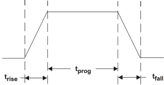
  Figure 11. OTP Programming Pulse Detail