SLUU254A December 2006 – January 2022 TPS40075
- Trademarks
- 1Introduction
- 2TPS40075EVM-001 Electrical Performance Specifications
- 3Schematic
- 4Test Setup
- 5TPS40075EVM Typical Performance Data and Characteristic Curves
- 6EVM Assembly Drawings and Layout
- 7List of Materials
- 8Revision History
3.1 Adjusting Output Voltage (R5 and R6)
The regulated output voltage can be adjusted within a limited range by changing the ground resistor in the feedback resistor divider (R6 and R5). The output voltage is given by Equation 1.
Equation 1. 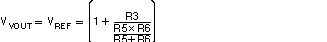
where
- VVREF = 0.700 V
- R3 = 10.0 kΩ
Table 3-1 contains common values for R6 to generate popular output voltages with R5 open R5 can be used to increase the accuracy that can be obtained without using more expensive resistors. The TPS40075EVM-001 is stable through these output voltages but the efficiency can suffer as the power stage is optimized for the 1.5-V output.
Table 3-1 Adjusting V1V5_OUT With R14
| VOUT (V) | R16 (kΩ) |
|---|---|
| 3.3(1) | 2.67 |
| 2.5(1) | 3.83 |
| 2.2(1) | 4.64 |
| 2.0(1) | 8.36 |
| 1.8 | 6.34 |
| 1.5 | 8.66 |
| 1.2 | 14.0 |
(1) Due to higher duty cycles associated with higher output voltages or lower input
voltages, output current should be limited to 10 A when operating with output voltages
greater than 2.0 V or input voltages below 6 V to reduce conduction losses in the main
switching FET (Q1). Under these conditions, a lower R(DS)on FET would normally
be selected.