SLUU381B September   2009  – February 2022 TPS51220A


  1.   Trademarks
  2. Introduction
  3. Description
    1. 2.1 Typical Applications
    2. 2.2 Features
  4. Electrical Performance Specifications
  5. Schematic
  6. Test Setup
    1. 5.1 Test Equipment
    2. 5.2 Recommended Test Setup
    3. 5.3 List of Test Points
  7. Test Procedure
    1. 6.1 Line/Load Regulation and Efficiency Measurement Procedure
    2. 6.2 Output Ripple Test
    3. 6.3 Measuring Improved Light Load Efficiency
    4. 6.4 Control Architecture and OVP Select
    5. 6.5 Overcurrent Trip Level and Output Discharge Select
  8. Performance Data and Typical Characteristic Curves
    1. 7.1 Efficiency
    2. 7.2 Load Regulation
    3. 7.3 Bode Plot
    4. 7.4 Transient Response
    5. 7.5 Output Ripple and Switch Node
    6. 7.6 Turn-On Waveform
    7. 7.7 Turn-Off Waveform
  9. EVM Assembly Drawing and PCB Layout
  10. List of Materials
  11. 10Revision History

EVM Assembly Drawing and PCB Layout

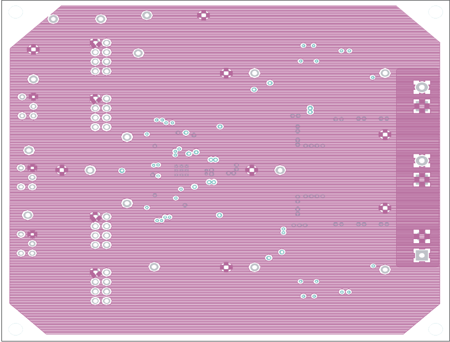
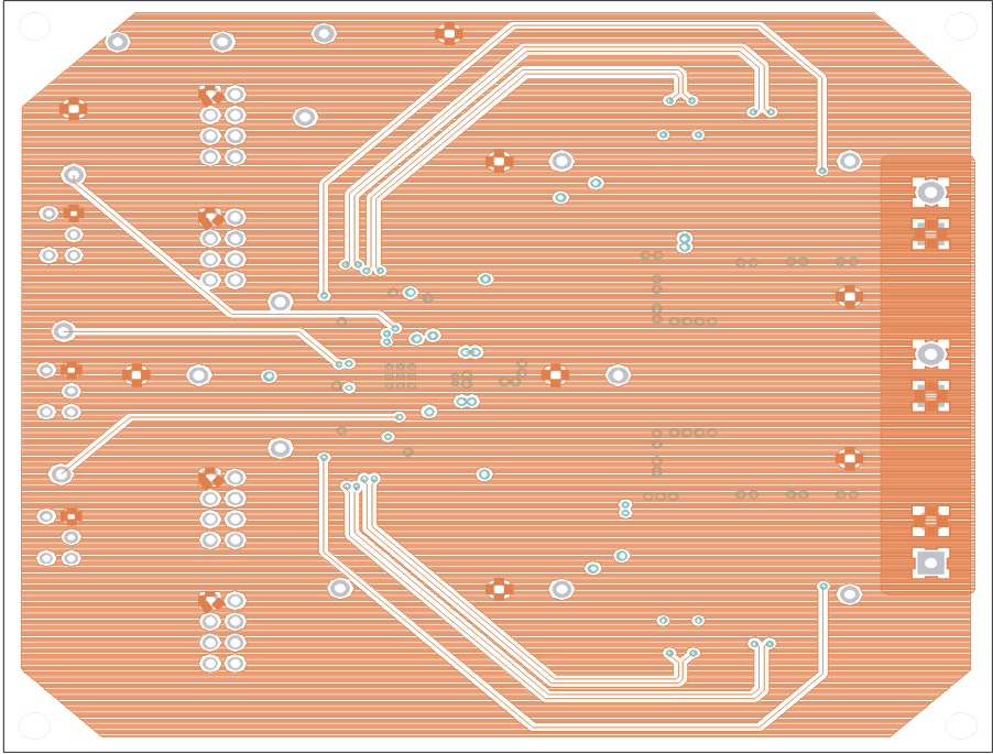
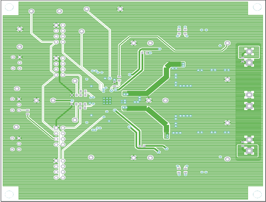
The following figures (Figure 8-1 through Figure 8-6) show the design of the TPS51220A EVM-476 printed circuit board. The PCB is 0.062” thick. It uses four layers of copper. The two internal layers are 2-oz copper while the external layers are 1-oz copper.
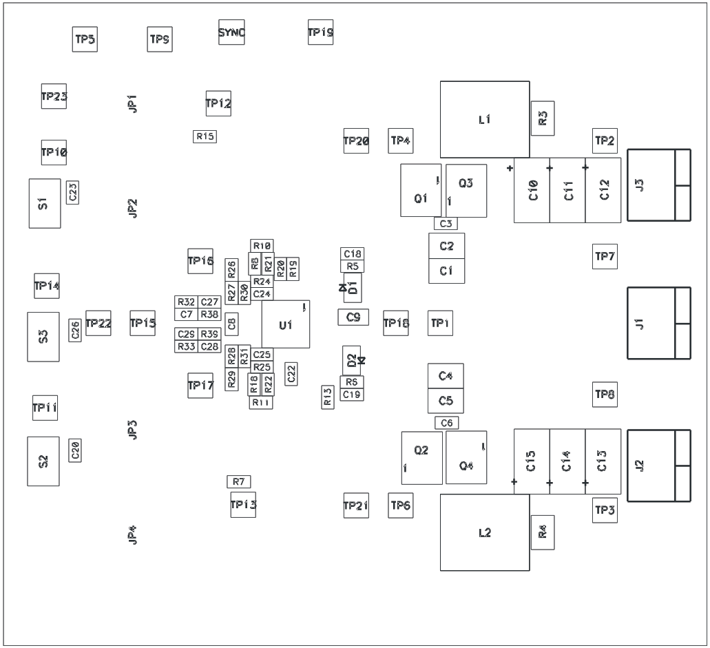
GUID-5B1CAAC9-3CBC-45B7-9485-9F6403295265-low.gifFigure 8-1 Top Layer Assembly Drawing (Top View)
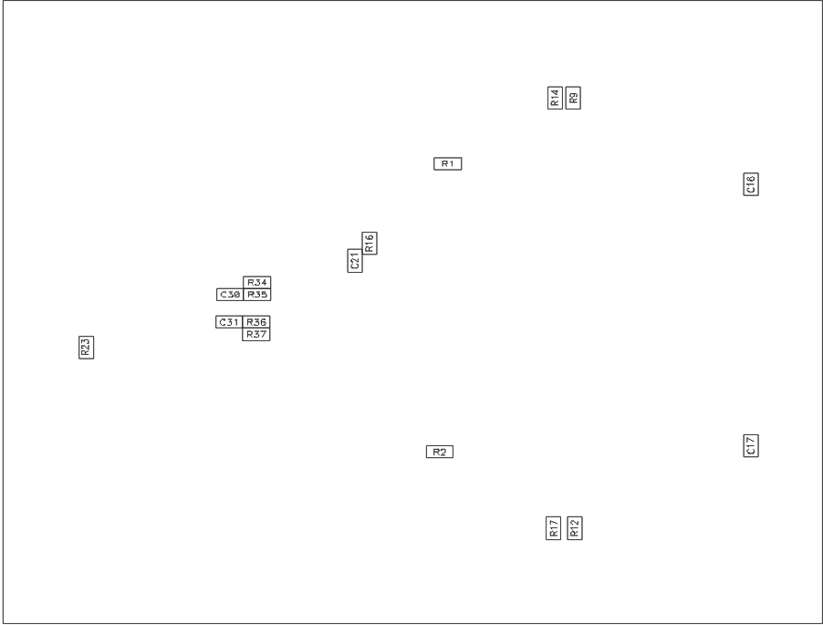
GUID-EF2DF2E5-1504-493D-938E-6C06DC017F9B-low.gifFigure 8-2 Bottom Assembly Drawing (Top View)
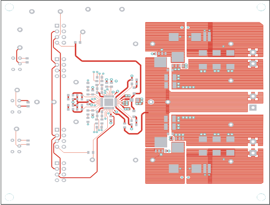
GUID-C4A62C3E-2291-4D93-808E-CC4D57E8A85F-low.gifFigure 8-3 Top Copper (Top View)
GUID-4551AD6D-7FB6-4281-86C2-85514368774C-low.gifFigure 8-4 Internal Layer 1 (Top View)
GUID-3E3B4E8D-DA54-40E7-A9EC-12500CE3DE31-low.gifFigure 8-5 Internal Layer 2 (Top View)
GUID-88656123-F71B-4C0A-A6B5-669C1C1ED573-low.gifFigure 8-6 Bottom Copper (Top View)