SLUUA65E april 2014 – june 2023 BQ28Z610
- 1
- Read This First
- 1 Introduction
-
2 Protections
- 2.1 Introduction
- 2.2 Cell Undervoltage Protection
- 2.3 Cell Overvoltage Protection
- 2.4 Overcurrent in Charge Protection
- 2.5 Overcurrent in Discharge Protection
- 2.6 Hardware-Based Protection
- 2.7 Temperature Protections
- 2.8 Overtemperature in Charge Protection
- 2.9 Overtemperature in Discharge Protection
- 2.10 Undertemperature in Charge Protection
- 2.11 Undertemperature in Discharge Protection
- 2.12 Precharge Timeout Protection
- 2.13 Fast Charge Timeout Protection
-
3 Permanent Fail
- 3.1 Introduction
- 3.2 Safety Cell Overvoltage Permanent Fail
- 3.3 Voltage Imbalance at Rest Permanent Fail
- 3.4 Voltage Imbalance Active Permanent Fail
- 3.5 Charge FET Permanent Failure
- 3.6 Discharge FET Permanent Failure
- 3.7 Instruction Flash (IF) Checksum Permanent Fail
- 3.8 Data Flash (DF) Permanent Fail
-
4 Advanced Charge Algorithm
- 4.1 Introduction
- 4.2 Charge Temperature Ranges
- 4.3 Voltage Range
- 4.4 Charging Current
- 4.5 Charging Voltage
- 4.6 Valid Charge Termination
- 4.7 Charge and Discharge Alarms
- 4.8 Terminate Charge and Discharge Alarms
- 4.9 Precharge
- 4.10 Maintenance Charge
- 4.11 BROADCAST Mode
- 4.12 Charge Disable and Discharge Disable
- 4.13 Charge Inhibit
- 4.14 Charge Suspend
- 5 Power Modes
- 6 Gauging
- 7 Cell Balancing
- 8 Lifetime Data Collection
- 9 Device Security
- 10Manufacture Production
- 11Calibration
-
12I2C Commands
- 12.1
Standard Data Commands
- 12.1.1 0x00/01 ManufacturerAccess() Control
- 12.1.2 0x02/03 AtRate()
- 12.1.3 0x04/05 AtRateTimeToEmpty()
- 12.1.4 0x06/07 Temperature()
- 12.1.5 0x08/09 Voltage()
- 12.1.6 0x0A/0B BatteryStatus()
- 12.1.7 0x0C/0D Current()
- 12.1.8 0x0E/0F MaxError()
- 12.1.9 0x10/11 RemainingCapacity()
- 12.1.10 0x12/13 FullChargeCapacity()
- 12.1.11 0x14/15 AverageCurrent()
- 12.1.12 0x16/17 AverageTimeToEmpty()
- 12.1.13 0x18/19 AverageTimeToFull()
- 12.1.14 0x1A/1B StandbyCurrent()
- 12.1.15 0x1C/1D StandbyTimeToEmpty()
- 12.1.16 0x1E/1F MaxLoadCurrent()
- 12.1.17 0x20/21 MaxLoadTimeToEmpty()
- 12.1.18 0x22/23 AveragePower()
- 12.1.19 0x24/25 BTPDischargeSet()
- 12.1.20 0x26/27 BTPChargeSet()
- 12.1.21 0x28/29 InternalTemperature()
- 12.1.22 0x2A/2B CycleCount()
- 12.1.23 0x2C/2D RelativeStateOfCharge()
- 12.1.24 0x2E/2F State-of-Health (SOH)
- 12.1.25 0x30/31 ChargingVoltage()
- 12.1.26 0x32/33 ChargingCurrent()
- 12.1.27 0x3C/3D DesignCapacity()
- 12.1.28 0x3E/3F AltManufacturerAccess()
- 12.1.29 0x40/0x5F MACData()
- 12.1.30 0x60 MACDataChecksum()
- 12.1.31 0x61 MACDataLength()
- 12.2
0x00, 0x01 AltManufacturerAccess() and 0x3E, 0x3F AltManufacturerAccess()
- 12.2.1 AltManufacturerAccess() 0x0001 Device Type
- 12.2.2 AltManufacturerAccess() 0x0002 Firmware Version
- 12.2.3 AltManufacturerAccess() 0x0003 Hardware Version
- 12.2.4 AltManufacturerAccess() 0x0004 Instruction Flash Signature
- 12.2.5 AltManufacturerAccess() 0x0005 Static DF Signature
- 12.2.6 AltManufacturerAccess() 0x0006 Chemical ID
- 12.2.7 AltManufacturerAccess() 0x0007 Pre_MACWrite
- 12.2.8 AltManufacturerAccess() 0x0008 Static Chem DF Signature
- 12.2.9 AltManufacturerAccess() 0x0009 All DF Signature
- 12.2.10 AltManufacturerAccess() 0x0010 SHUTDOWN Mode
- 12.2.11 AltManufacturerAccess() 0x0011 SLEEP Mode
- 12.2.12 AltManufacturerAccess() 0x0012 Device Reset
- 12.2.13 AltManufacturerAccess() 0x001F CHG FET
- 12.2.14 AltManufacturerAccess() 0x0020 DSG FET
- 12.2.15 AltManufacturerAccess() 0x0021 Gauging
- 12.2.16 AltManufacturerAccess() 0x0022 FET Control
- 12.2.17 AltManufacturerAccess() 0x0023 Lifetime Data Collection
- 12.2.18 AltManufacturerAccess() 0x0024 Permanent Failure
- 12.2.19 AltManufacturerAccess() 0x0028 Lifetime Data Reset
- 12.2.20 AltManufacturerAccess() 0x0029 Permanent Fail Data Reset
- 12.2.21 AltManufacturerAccess() 0x002D CALIBRATION Mode
- 12.2.22 AltManufacturerAccess() 0x0030 Seal Device
- 12.2.23 AltManufacturerAccess() 0x0035 Security Keys
- 12.2.24 AltManufacturerAccess() 0x0037 Authentication Key
- 12.2.25 AltManufacturerAccess() 0x0041 Device Reset
- 12.2.26 AltManufacturerAccess() 0x0050 SafetyAlert
- 12.2.27 AltManufacturerAccess() 0x0051 SafetyStatus
- 12.2.28 AltManufacturerAccess() 0x0052 PFAlert
- 12.2.29 AltManufacturerAccess() 0x0053 PFStatus
- 12.2.30 AltManufacturerAccess() 0x0054 OperationStatus
- 12.2.31 AltManufacturerAccess() 0x0055 ChargingStatus
- 12.2.32 AltManufacturerAccess() 0x0056 GaugingStatus
- 12.2.33 AltManufacturerAccess() 0x0057 ManufacturingStatus
- 12.2.34 AltManufacturerAccess() 0x0058 AFE Register
- 12.2.35 AltManufacturerAccess() 0x0060 Lifetime Data Block 1
- 12.2.36 AltManufacturerAccess() 0x0070 ManufacturerInfo
- 12.2.37 AltManufacturerAccess() 0x0071 DAStatus1
- 12.2.38 AltManufacturerAccess() 0x0072 DAStatus2
- 12.2.39 AltManufacturerAccess() 0x0073 ITStatus1
- 12.2.40 AltManufacturerAccess() 0x0074 ITStatus2
- 12.2.41 AltManufacturerAccess() 0x0075 ITStatus3
- 12.2.42 AltManufacturerAccess() 0x0076 CB Status
- 12.2.43 AltManufacturerAccess() 0x0077 State-of-Health
- 12.2.44 AltManufacturerAccess() 0x0F00 ROM Mode
- 12.2.45 Data Flash Access() 0x4000–0x5FFF
- 12.2.46 AltManufacturerAccess() 0xF080 Exit Calibration Output Mode
- 12.2.47 AltManufacturerAccess() 0xF081 Output CC and ADC for Calibration
- 12.2.48 AltManufacturerAccess() 0xF082 Output Shorted CC and ADC for Calibration
- 12.1
Standard Data Commands
-
13Data Flash Values
- 13.1 Data Formats
- 13.2 Calibration
- 13.3 Settings
- 13.4 Advanced Charging Algorithms
- 13.5 Power
- 13.6 Gas Gauging
- 13.7 System Data
- 13.8 Configuration
- 13.9 Lifetimes
- 13.10
Protections
- 13.10.1 CUV—Cell Undervoltage
- 13.10.2 COV—Cell Overvoltage
- 13.10.3 OCC—Overcurrent In Charge
- 13.10.4 OCD—Overcurrent In Discharge
- 13.10.5 AOLD—AFE Over Load In Discharge
- 13.10.6 ASCC—AFE Short Circuit in Charge
- 13.10.7 ASCD—AFE Short Circuit in Discharge
- 13.10.8 OTC—Overtemperature in Charge
- 13.10.9 OTD—Overtemperature in Discharge
- 13.10.10 UTC—Under Temperature in Charge
- 13.10.11 UTD—Under Temperature in Discharge
- 13.10.12 PTO—PRECHARGE Mode Time Out
- 13.10.13 CTO—FAST CHARGE Mode Time Out
- 13.11 Permanent Fail
- 13.12 PF Status
- 13.13 RA Table
- 14Data Flash Summary
- A AFE Threshold and Delay Settings
- B Revision History
7.2 Cell Balancing Setup
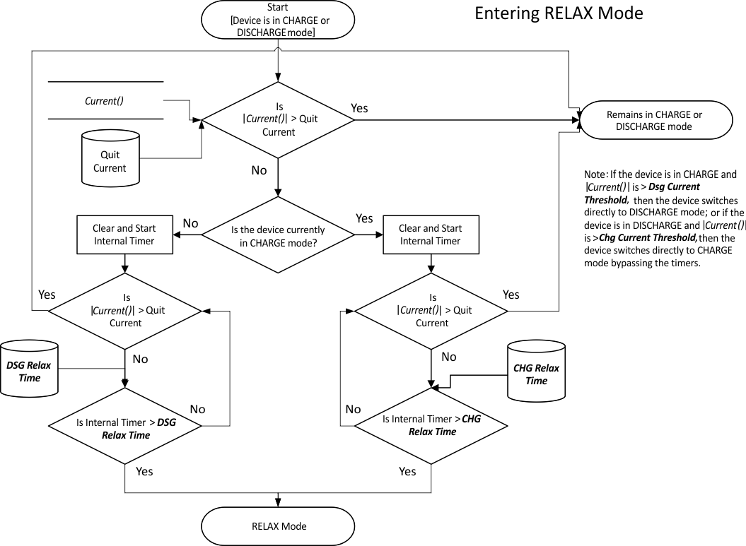
The BQ28Z610 is required to be in RELAX mode before it can check if the cells are unbalanced and how much balancing is required. The BQ28Z610 enters RELAX mode when:
Current() < Quit Current for at least Dsg Relax Time when coming from DISCHARGE mode for Chg Relax Time when coming for CHARGE mode.
 Figure 7-1 Entering CHARGE or RELAX Mode
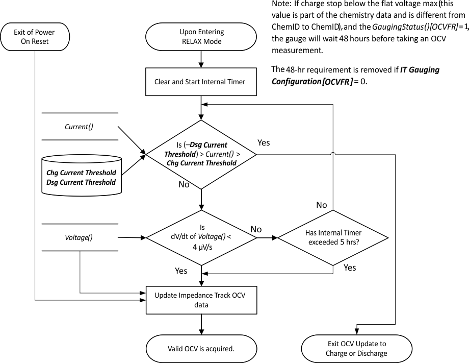
Once in RELAX mode, the BQ28Z610 waits until an OCV measurement is taken, which occurs after:
- A dV/dt condition of < 4 µV/s is satisfied,
- After 5 hours from when Current() < Quit Current,
- Upon gas gauge reset,
- An IT Enable command is issued.
The determination of when to update the OCV data is part of the normal Impedance Track algorithm and is not specific to the cell balancing algorithm.
 Figure 7-2 OCV Measurement
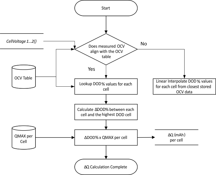
The BQ28Z610 then calculates the amount of charge difference between cells with a higher state-of-charge than the lowest cell SOC. The value, dQ, is determined for each cell based by converting the measured OCV to Depth-of-Discharge (DOD) percentages using a temperature-compensated DOD vs. OCV table lookup table. If the measured, OCV does not coincide with a specific table entry, then the DOD value is linearly interpolated from the two adjacent DODs of the respective table adjacent OCVs.
The delta in DOD% between each cell and the cell of lowest SOC is multiplied by the respective cells QMax to create dQ: for example, dQ = CellnDOD – CellLOWEST_SOC DOD × CellnQMax (mAh).
 Figure 7-3 ΔQ Calculation
The BQ28Z610 calculates the required balancing time using dQ and Bal Time/mAh Cell 1 (for cell 1) or Bal Time/mAh Cell 2. The value of Bal Time/mAh Cell 1 and Bal Time/mAh Cell 2 is fixed based on key system factors and is calculated by:
Bal Time/mAh Cell x = 3600 mAs/(DUTY × (1000 mV / 1 V) × VCELL/(RVCx + Rcb))
Where:
VCELL = average cell voltage (for example, 3.7 V for most chemistry)
RVCx = external resistance in series between the cell and the pins of the BQ28Z610. In the reference schematic, RVC2 = 105 Ω and RVC1 = 100 Ω.
Rcb = cell balancing FET Rdson, which is 150 Ω.
DUTY = cell balancing duty cycle, which is 68.75% typ.
Cell balancing time for each cell to be balanced is calculated by: dQCelln × Bal Time/mAh Cell 1 for cell1 or and dQCelln × Bal Time/mAh Cell 2. The cell balancing time is stored in the 16-bit RAM register CellnBalanceTimer, providing a maximum calculated time of 65535 s (or 18.2 hrs). This update only occurs if a valid QMax update has been made; otherwise, they are all set to 0.
The CellnBalanceTimer registers are clamped at 0xFFFF and cannot roll over.