SLUUBW8A July 2018 – February 2022 TPS543C20
- Trademarks
- 1 Introduction
- 2 Description
- 3 EVM Electrical Performance Specifications
- 4 Schematic
- 5 Test Equipment
- 6 BSR054EVM
- 7 List of Test Points, Jumpers, and Switch
- 8 Test Procedure
- 9 Performance Data and Typical Characteristic Curves
- 10EVM Assembly Drawing and PCB Layout
- 11List of Materials
- 12Revision History
10 EVM Assembly Drawing and PCB Layout
Figure 10-1 through Figure 10-8 show the design of the BSR054EVM printed-circuit board (PCB). The BSR054EVM has a 2-oz. copper finish for all layers.
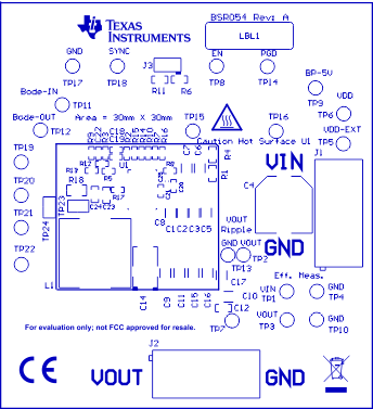 Figure 10-1 BSR054EVM
Top Layer Assembly Drawing (Top View)
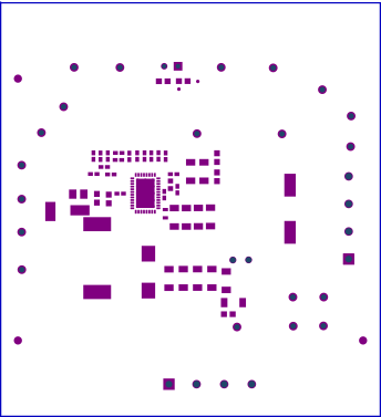 Figure 10-2 BSR054EVM
Top Solder Mask (Top View)
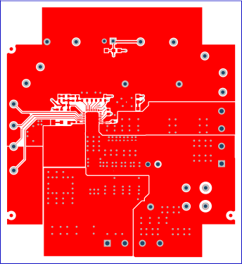 Figure 10-3 BSR054EVM
Top Layer (Top View)
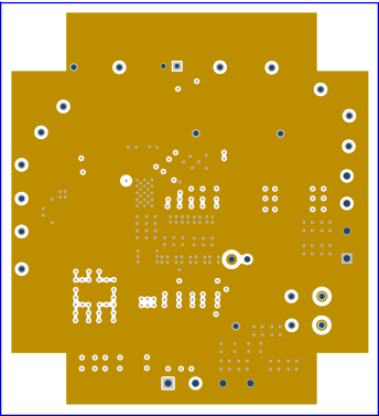 Figure 10-4 BSR054EVM
Inner Layer 1 (Top View)
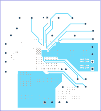 Figure 10-5 BSR054EVM
Inner Layer 2 (Top View)
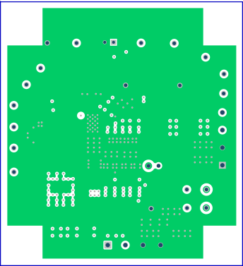 Figure 10-6 BSR054EVM
Inner Layer 3 (Top View)
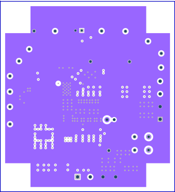 Figure 10-7 BSR054EVM
Inner Layer 4 (Top View)
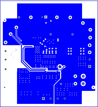 Figure 10-8 BSR054EVM
Bottom Layer (Top View)
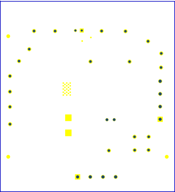 Figure 10-9 BSR054EVM
Bottom Solder Mask (Top View)
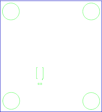 Figure 10-10 BSR054EVM
Bottom Overlay Layer (Top View)