SLUUC03A February 2019 – December 2022 TPS566235
6.1 Power Up
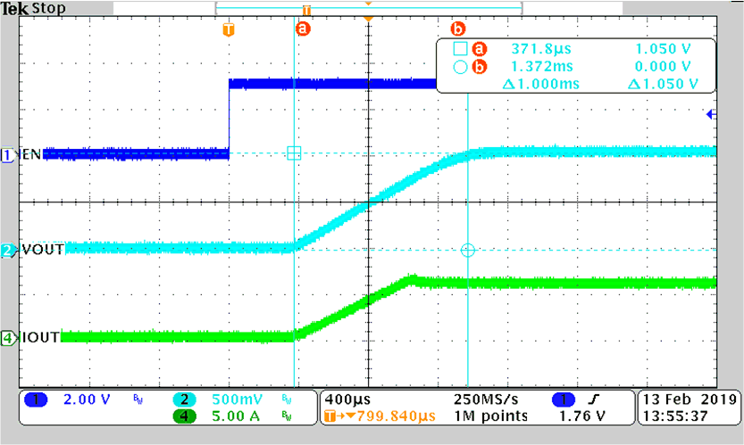
Figure 6-1 shows the power up waveform at 12-V input and 1.05-V output. Once the EN signal is high, VOUT starts to ramp up.
 Figure 6-1 Power up with 6 A loading controlled by EN pin
SLUUC03A February 2019 – December 2022 TPS566235
Figure 6-1 shows the power up waveform at 12-V input and 1.05-V output. Once the EN signal is high, VOUT starts to ramp up.
 Figure 6-1 Power up with 6 A loading controlled by EN pin