SLVA997A November 2018 – July 2021 TPS61322
4 Bench Result
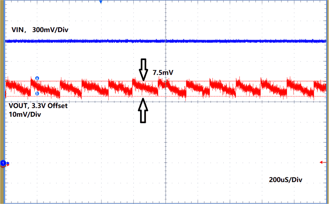
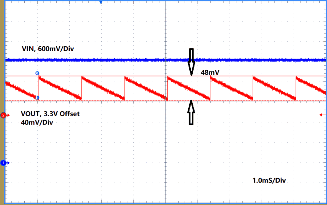
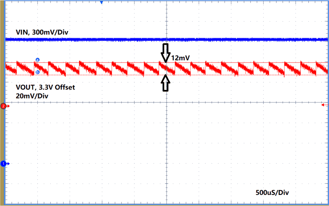
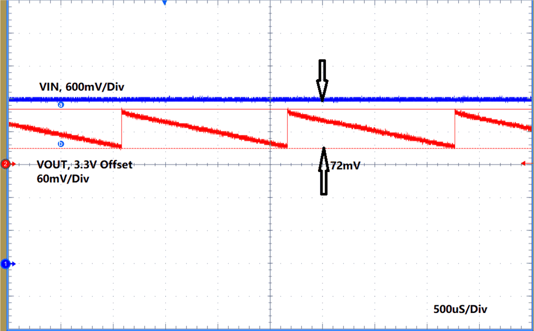
Different output capacitors are used to verify the single pulse power-save mode.
 Figure 4-1 VIN = 1.8 V, COUT = 10 µF
 Figure 4-3 VIN = 3 V, COUT = 10 µF
 Figure 4-2 VIN = 1.8 V, COUT = 4.7 µF
 Figure 4-4 VIN = 3 V, COUT = 4.7 µF
| VIN | LOAD | C1 = 4.7 µF | C1 = 10 µF |
|---|---|---|---|
| 3 V | 100 µA | 71.58 | 48.52 |
| 1 mA | 71.58 | 48.52 | |
| 10 mA | 29.79 | 18.26 | |
| 1.8 V | 100 µA | 12.26 | 7.53 |
| 1 mA | 11.86 | 7.53 | |
| 10 mA | 20.26 | 11.33 | |
| 0.9 V | 100 µA | 7.86 | 7.53 |
| 1 mA | 7.86 | 7.53 | |
| 10 mA | 46.92 | 23.46 |
From the typical application curves and the output ripple values listed in the table, the output ripple of TPS613221A is 7.5 mV and 48.5 mV when the output capacitor is 10 µF (The actual output capacitance is 7 µF under 3.3-V bias voltage ). While it increases to 12 mV and 72 mV if the output capacitor is modified to 4.7 µF (the actual capacitance is 3.6 µF under 3.3-V bias voltage)
As the comparison, the traditional power save mode introduces more than 0.8% × VOUT output ripple. It is much higher than the single-pulse, power-save-mode control method if the TPS61021A has all the same output capacitance, inductance and internal comparator delay time as that of TPS613221A. Another one or two pulses will be introduced even the output voltage triggers the 1.008 × VOUT threshold. That means the output ripple can reaches 34 mV or more when the output voltage is 10uF. This becomes even worse when the input voltage is 3 V because a single pulse introduces 48-mV output ripple. That means for some cycles, the output ripple can be as high as 83 mV.