SLVAE30E February 2021 – March 2021 TPS1H000-Q1 , TPS1H100-Q1 , TPS1H200A-Q1 , TPS1HA08-Q1 , TPS25200-Q1 , TPS27S100 , TPS2H000-Q1 , TPS2H160-Q1 , TPS2HB16-Q1 , TPS2HB35-Q1 , TPS2HB50-Q1 , TPS4H000-Q1 , TPS4H160-Q1
- Trademarks
- 1Introduction
- 2Driving Resistive Loads
- 3Driving Capacitive Loads
- 4Driving Inductive Loads
- 5Driving LED Loads
- 6Appendix
- 7References
- 8Revision History
3.3.5 Over Temperature Shutdown
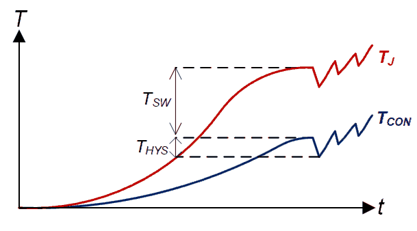
To ensure there are no failures during high power dissipation, TI Smart High Side Switches integrate two methods of over temperature protection. The first is an absolute thermal shutdown that turns off the FET when the junction temperature reaches an unsafe level, typically around 150°C. The second is a relative thermal shutdown, or thermal swing shutdowthat measures the temperature difference between the FET and the controller. This will shut the Smart High Side Switch off during large transients where the FET quickly heats up but the controller lags the FET temperature. This protection increases reliability in two primary cases:
- Protection against localized hot spots in the FET that are not recorded by the temperature sensor. With only an absolute temperature shutdown you are assuming that the measurement is occurring at the hottest part of the junction, which cannot be guaranteed.
- Protection in short circuit situations with cable inductance. During an output short circuit the output wants to draw very high currents so the Smart High Side Switch will clamp at the current limit until it hits thermal shutdown. Once thermal shutdown is hit the output current will immediately stop, however any output inductance that is present in a cable will attempt to continue the current flow and the Smart High Side Switch must demagnetize this inductance. For more details on demagnetizing inductive loads reference Section 4. If the Smart High Side Switch is already at its peak junction temperature this demagnetization energy will destroy the switch. By using the relative temperature of the FET to register this short circuit and shut the device down earlier the device ensures it is capable of absorbing the demagnetization energy safely.
 Figure 3-17 Thermal Cycling due to relative thermal shutdown mechanism
When either of these shutdown mechanisms occurs, the switch shuts off to prevent current flow to the load. By preventing current to the load, the device prevents any additional power dissipation in the Smart High Side Switch. This gives the switch time to cool down and reach a safe temperature.
During the shutdown the open FET temporarily prevents the capacitor from charging, however TI Smart High Side Switches have a fast cool-down and retry time so the charge erosion on the capacitor will be limited and upon restart the switch will continue charging. This means that if the Smart High Side Switch hits thermal shutdown it will quickly try again and resume charging the capacitor safely.
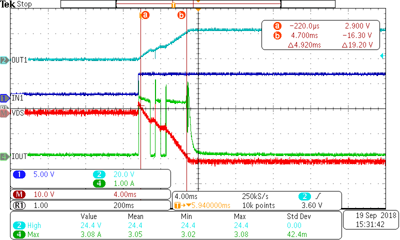
This behavior can be seen in Figure 3-18 where the TPS2H160-Q1 drives 470µF to 24V with a current limit of 2.2A. It can be observed that on two occasions the device reaches the relative temperature shutdown and temporarily disables the switch preventing current flow before re-enabling after the device has had a chance to cool down. In this way, the TI Smart High Side Switch protects itself from over-temperature stresses when driving large capacitive loads.
 Figure 3-18 TPS2H160-Q1 Thermal Shutdown While Driving Capacitance
This analysis is important to understand while selecting a TI device for driving capacitive loads. Ideally, the Smart High Side Switch should be able to drive the load without any shutdowns, however a designer should balance the current limit set-point with the required charging time. To determine whether the device will go into thermal shutdown the best method is to test the specific load profile with a TI evaluation module, but for a detailed analysis an RC thermal model can also be used.