SLVAEW7 September   2020 ADC12DJ5200RF , LMK00304 , LMK04828 , LMX2594 , TPS62912 , TPS62913


  1.   Trademarks
  2. 1Introduction and System Description
    1. 1.1 Introduction
      1. 1.1.1 ADC12DJ5200 Noise and Ripple Requirements
      2. 1.1.2 Power Supply Requirements for Wideband RF PLL and Clocks
      3. 1.1.3 TPS62913 Low-Noise and Low-Ripple Buck Converter
    2. 1.2 Block Diagram
    3. 1.3 Design Considerations
  3. 2Tests and Results
    1. 2.1 Test Methodology
    2. 2.2 Test Conditions
    3. 2.3 Test Results
  4. 3Conclusion
  5. 4References
  6. 5Appendix

Appendix

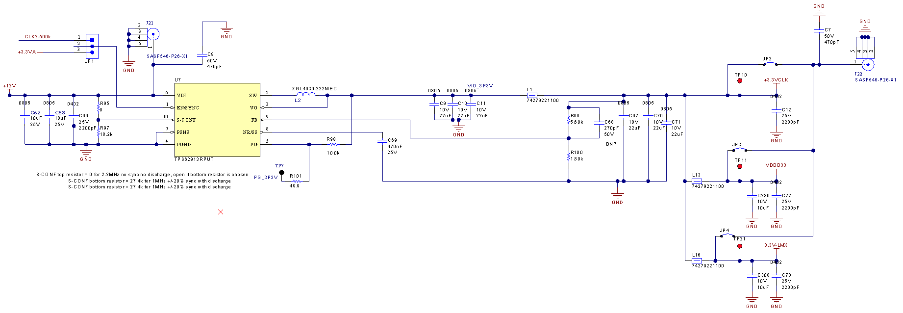
GUID-20200914-CA0I-K1SD-NMJV-RG2LPLMRMC8L-low.gif Figure 5-1 TPS62913 3.3V Clock Power Schematic
GUID-20200914-CA0I-FSHZ-WZBP-FDLBFXRJCBLN-low.gif Figure 5-2 TPS6913 VA11 ADC Power Schematic
GUID-20200914-CA0I-MNP6-N5QM-CNFRH5SQNJL5-low.gif Figure 5-3 TPS62913 VD11 ADC Power Schematic
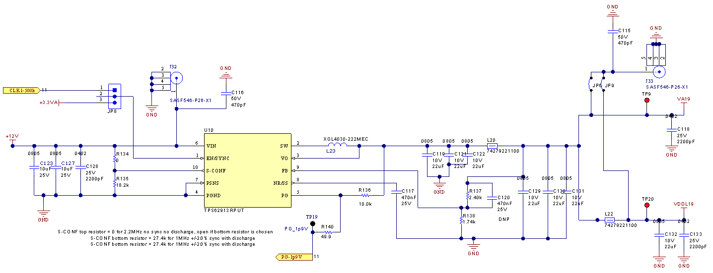
GUID-20200914-CA0I-27XF-TLR6-5B3D9XFX50P3-low.gif Figure 5-4 TPS62913 VA19 ADC Power Schematic