SLVSAX2B September 2011 – June 2020 TPS61170-Q1
PRODUCTION DATA.
- 1 Features
- 2 Applications
- 3 Description
- 4 Revision History
- 5 Pin Configuration and Functions
- 6 Specifications
- 7 Detailed Description
-
8 Application and Implementation
- 8.1 Application Information
- 8.2 Typical Applications
- 9 Power Supply Recommendations
- 10Layout
- 11Device and Documentation Support
- 12Mechanical, Packaging, and Orderable Information
7.5.1 Feedback Reference Program Mode Selection
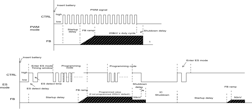
The CTRL pin is used for changing the FB pin reference voltage on-the-fly. There are two methods to program the reference voltage, PWM signal and 1-wire interface (EasyScale). The programming mode is selected each time the device is enabled. The default mode is to use the duty cycle of the PWM signal on the CTRL pin to modulate the reference voltage. To enter the 1-wire interface mode, the following digital pattern on the CTRL pin must be recognized by the IC every time the IC starts from the shutdown mode.
- Pull CTRL pin high to enable the TPS61170-Q1 and to start the 1-wire mode detection window.
- After the EasyScale detection delay (tes_delay, 100 μsec) expires, drive CTRL low for more than the EasyScale detection time (tes_detect, 260 μsec).
- The CTRL pin must be low for more than EasyScale detection time before the EasyScale detection window (tes_win, 1ms) expires. EasyScale detection window starts from the first CTRL pin low to high transition.
The IC immediately enters the 1-wire mode once the preceding three conditions are met. The EasyScale communication can start before the detection window expires. Once the mode is programmed, it cannot be changed without another start-up. In other words, the IC must be shut down by pulling the CTRL low for 2.5 ms and restarted to exit EasyScale Mode. See Figure 14 for a graphical explanation.
 Figure 14. Mode Detection of Feedback Reference Program