SLVU097B October 2003 – October 2021 TPS54350
2.2 Efficiency
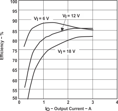
The TPS54350EVM−235 efficiency peaks at load current of approximately 1 A and VI of 6 V, and then decreases as the load current increases towards full load. For higher input voltages, quiescent losses are greater and the efficiency peaks under full load conditions. It is important to consider that this design is optimized for small size and flexibility and does not reflect the high efficiencies that are possible for specific applications using the TPS54350. Figure 2-2 shows the efficiency for the TPS54350 at an ambient temperature of 250°C. The efficiency is lower at higher ambient temperatures, due to temperature variation in the drain-to-source resistance of the MOSFETs. The efficiency is slightly lower at 500 kHz than at lower switching frequencies due to the gate and switching losses in the MOSFETs.
 Figure 2-2 Measured Efficiency