SLVU189B february   2007  – may 2023 TPS74701 , TPS74801


  1.   1
  2.   Abstract
  3.   Trademarks
  4. 1Introduction
    1. 1.1 Performance Specification Summary
    2. 1.2 Modifications
  5. 2Input and Output Connector Descriptions
    1. 2.1  J1–VIN/GND
    2. 2.2  J2–GND
    3. 2.3  J3–VIN
    4. 2.4  J4–VBIAS
    5. 2.5  J5–GND
    6. 2.6  J6–VOUT
    7. 2.7  J7–GND
    8. 2.8  J8–VOUT/GND
    9. 2.9  J10–EN
    10. 2.10 J11–GND
    11. 2.11 J12-VIN/GND
    12. 2.12 J13-VOUT/GND
    13. 2.13 JP1–1 ms/Simult Versus 10 ms/Ratio
    14. 2.14 S1
    15. 2.15 TP1
    16. 2.16 TP2
    17. 2.17 TP3
    18. 2.18 TP4
  6. 3Test Setup
  7. 4Test Results
  8. 5Board Layout
  9. 6Bill of Materials and Schematic
    1. 6.1 Schematic Drawing
  10. 7Revision History

Board Layout

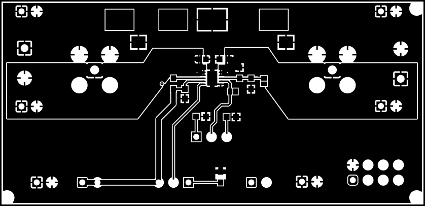
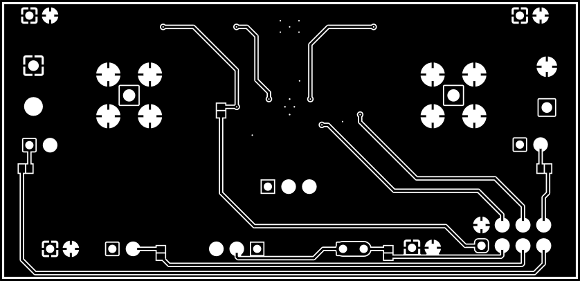
Board layout is important for improving power supply rejection ratio (PSRR) and lowering noise. Figure 5-1, Figure 5-2, Figure 5-3, and Figure 5-4 show the board layout for the HPA177 EVM. The switching nodes with high-frequency noise are isolated from the noise-sensitive feedback circuitry. See the data sheet for more specific layout guidelines.
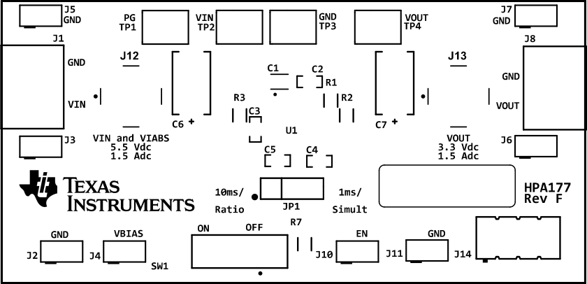
GUID-20230130-SS0I-N7WJ-D3MV-GF5FJGMTVVG6-low.gif Figure 5-1 Top Overlay
GUID-20230130-SS0I-CDV0-WF2F-BWPCDDPJL6XP-low.gif Figure 5-2 Top Layer
GUID-20230130-SS0I-3Q44-CVT4-SNQMZGPG1PCR-low.gif Figure 5-3 Bottom Layer
GUID-20230130-SS0I-44PC-MLHL-6XMNKG5NL4FZ-low.gif Figure 5-4 Bottom Overlay