SLVU251B June 2008 – February 2022 TPS51220
7 EVM Assembly Drawing and PCB Layout
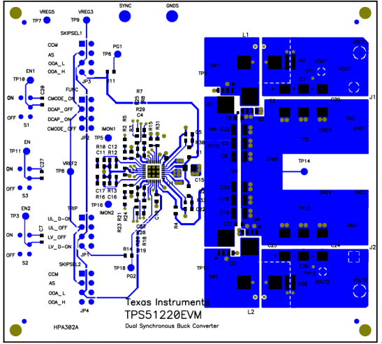 Figure 7-1 Top Layer/ Assembly
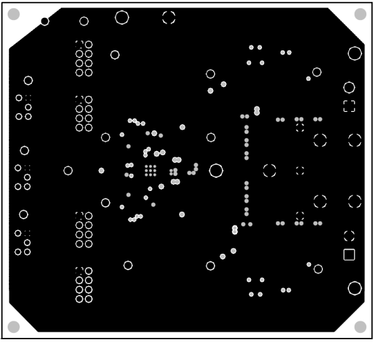 Figure 7-2 Inner Layer 1
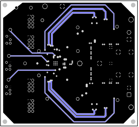 Figure 7-3 Inner Layer 2
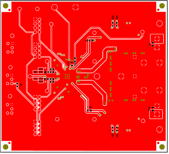 Figure 7-4 Bottom Layer/ Assembly
SLVU251B June 2008 – February 2022 TPS51220
 Figure 7-1 Top Layer/ Assembly
 Figure 7-2 Inner Layer 1
 Figure 7-3 Inner Layer 2
 Figure 7-4 Bottom Layer/ Assembly