SLVU641A January 2012 – November 2021 TPS54120
4.3 Output Turn-On
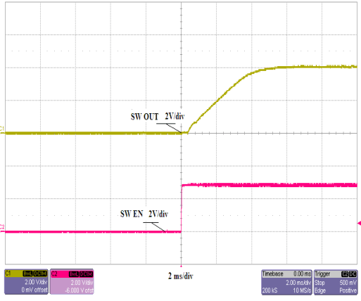
Figure 4-3 shows the SW output voltage turn-on from the SW enable for the TPS54120EVM with VIN = 12 V, SW OUT = 4.1 V, LDO OUT = 3.3 V, and IOUT = 400 mA, Fswitching = 480 kHz.
 Figure 4-3 Switcher Converter Output
Voltage Turn-On, SW Enable
Figure 4-3 Switcher Converter Output
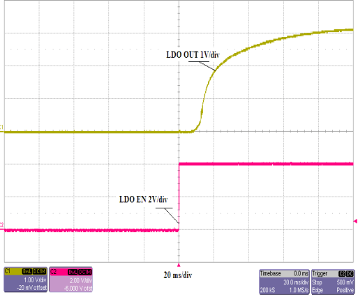
Voltage Turn-On, SW EnableFigure 4-4 shows the LDO output voltage turn-on from the LDO enable for the TPS54120EVM with VIN = 12 V, SW OUT = 4.1 V, LDO OUT = 3.3 V, and IOUT = 400 mA, Fswitching = 480 kHz.
 Figure 4-4 LDO Output Voltage
Turn-On, LDO Enable
Figure 4-4 LDO Output Voltage
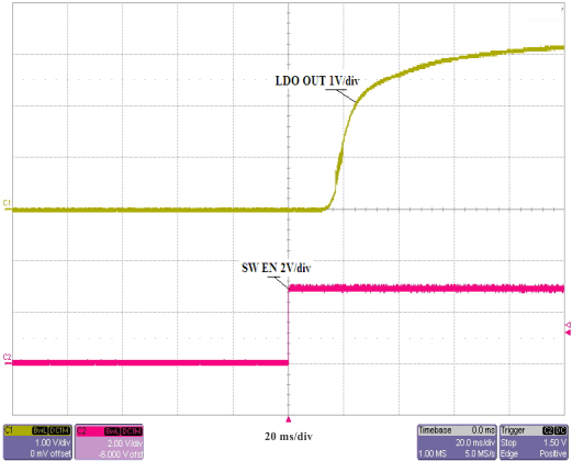
Turn-On, LDO EnableFigure 4-5 shows the LDO output voltage turn-on of TPS54120 from the SW enable for the TPS54120EVM with VIN = 12 V, SW OUT = 4.1 V, LDO OUT = 3.3 V, and IOUT = 400 mA, Fswitching = 480 kHz.
 Figure 4-5 LDO Output Voltage
Turn-On, SW Enable