SLVU735A June   2012  – February 2022 TPS51225


  1.   Trademarks
  2. Description
    1. 1.1 Typical Applications
    2. 1.2 Features
  3. Electrical Performance Specifications
  4. Schematic
  5. Test Setup
    1. 4.1 Test Equipment
    2. 4.2 Recommended Test Setup
  6. Configurations
  7. Test Procedure
    1. 6.1 Line/Load Regulation and Efficiency Measurement Procedure
    2. 6.2 List of Test Points
    3. 6.3 Equipment Shutdown
  8. Performance Data and Typical Characteristic Curves
    1. 7.1  5-V Efficiency
    2. 7.2  5-V Load Regulation
    3. 7.3  3.3-V Efficiency
    4. 7.4  3.3-V Load Regulation
    5. 7.5  Enable Turn-On/Turn-Off
    6. 7.6  Output Ripple
    7. 7.7  Switching Node
    8. 7.8  5-V Output Transient with Auto-skip Mode
    9. 7.9  3.3-V Output Transient with Auto-skip Mode
    10. 7.10 Output Prebias Turn-On
    11. 7.11 Thermal Image
  9. EVM Assembly Drawing and PCB Layout
  10. Bill of Materials
  11. 10Revision History

EVM Assembly Drawing and PCB Layout

The following figures (Figure 8-1 through Figure 8-6) show the design of the TPS51225EVM-133 printed circuit board. The EVM has been designed using four layers, 2-oz copper circuit board.
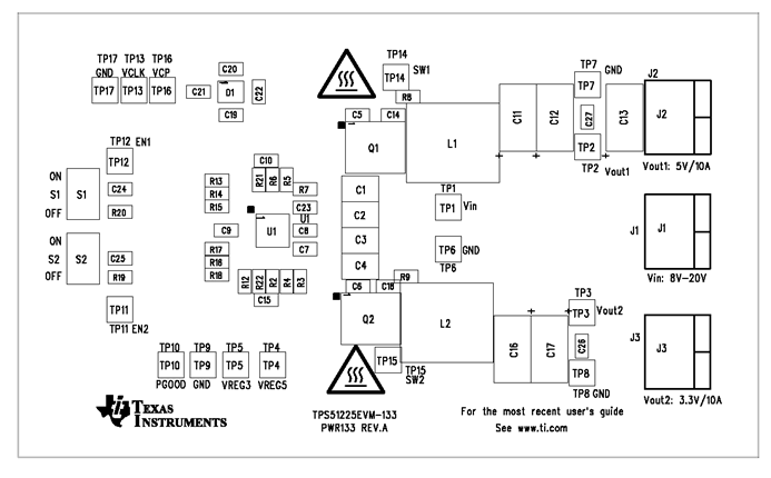
GUID-A289140D-551A-4036-AD03-C2D0B2E7DFFE-low.gifFigure 8-1 TPS51225EVM-133 Top Layer Assembly Drawing
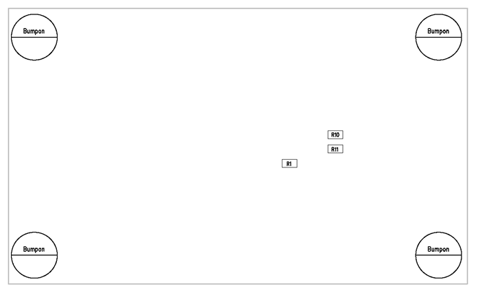
GUID-0A47515F-4E27-426B-B1DF-A4C68AA7BA36-low.gifFigure 8-2 TPS51225EVM-133 Bottom Assembly Drawing
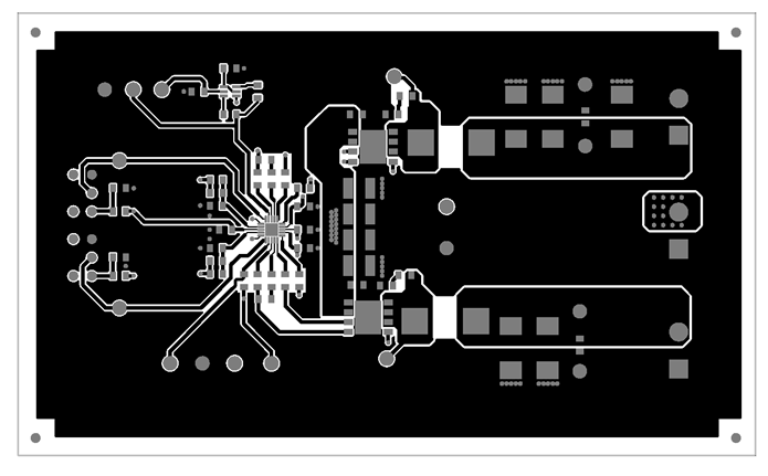
GUID-3062E912-3331-4A41-A07F-29FDC2091485-low.gifFigure 8-3 TPS51225EVM-133 Top Copper
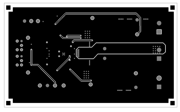
GUID-1AE43AFF-7992-4CFD-A56C-75503A380066-low.gifFigure 8-4 TPS51225EVM-133 Layer 2 Copper
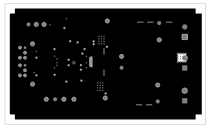
GUID-6DD7CD8D-F7A8-474B-AD3E-812511BF1A96-low.gifFigure 8-5 TPS51225EVM-133 Layer 3 Copper
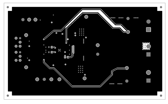
GUID-2AD5F7BE-CC6C-4657-91C3-D9D8F493241C-low.gifFigure 8-6 TPS51225EVM-133 Layer 4 Copper