SLVU793A October   2012  – June 2021 TPS56921


  1.   Trademarks
  2. 1Introduction
    1. 1.1 Background
    2. 1.2 Performance Specification Summary
    3. 1.3 Modifications
      1. 1.3.1 Output Voltage Setpoint
      2. 1.3.2 Slow-Start Time
      3. 1.3.3 Adjustable UVLO
      4. 1.3.4 Input Voltage Rails
  3. 2Test Setup and Results
    1. 2.1 Input/Output Connections
    2. 2.2 Efficiency
    3. 2.3 Output Voltage Load Regulation
    4. 2.4 Output Voltage Line Regulation
    5. 2.5 Load Transients
    6. 2.6 Loop Characteristics
    7. 2.7 Output Voltage Ripple
    8. 2.8 Input Voltage Ripple
    9. 2.9 Powering Up
  4. 3Board Layout
    1. 3.1 Layout
  5. 4Schematic and Bill of Materials
    1. 4.1 Schematic
    2. 4.2 Bill of Materials
  6. 5Revision History

Efficiency

Figure 2-1 shows the efficiency for the TPS56921EVM-188 at an ambient temperature of 25°C.
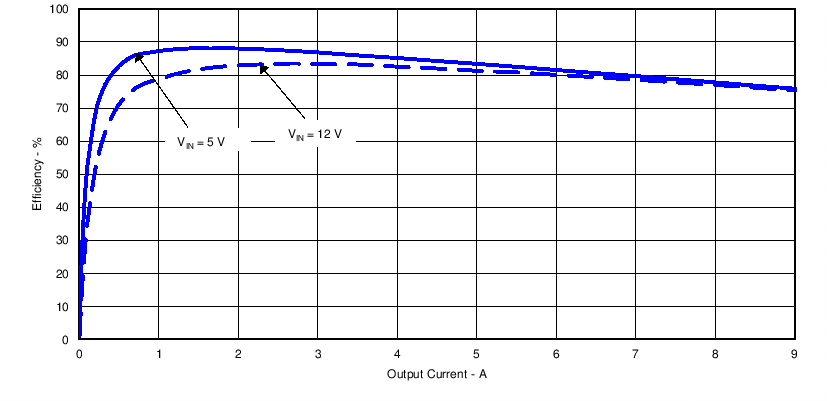
GUID-361B9F6D-B6B9-4D97-8C91-44ACD503DA09-low.pngFigure 2-1 TPS56921EVM-188 Efficiency

Figure 2-2 shows the efficiency for the TPS56921EVM-188 using a semi-log scale to more easily show efficiency at lower output currents. The ambient temperature is 25°C.
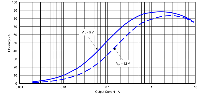
GUID-16EB9489-16B2-4E55-8E39-8126DEF02D3A-low.gifFigure 2-2 TPS56921EVM-188 Low Current Efficiency

The efficiency may be lower at higher ambient temperatures, due to temperature variation in the drain-to-source resistance of the internal MOSFET.