SLVUCF6 july 2023
- 1
- Abstract
- Trademarks
- 1Introduction
- 2Requirements
- 3TPS65219 Resources Overview
- 4EVM Configuration
- 5NVM Programming
- 6Graphical User Interface (GUI)
- 7Schematics, PCB Layouts, and Bill of Materials
6.5 Register Map Page
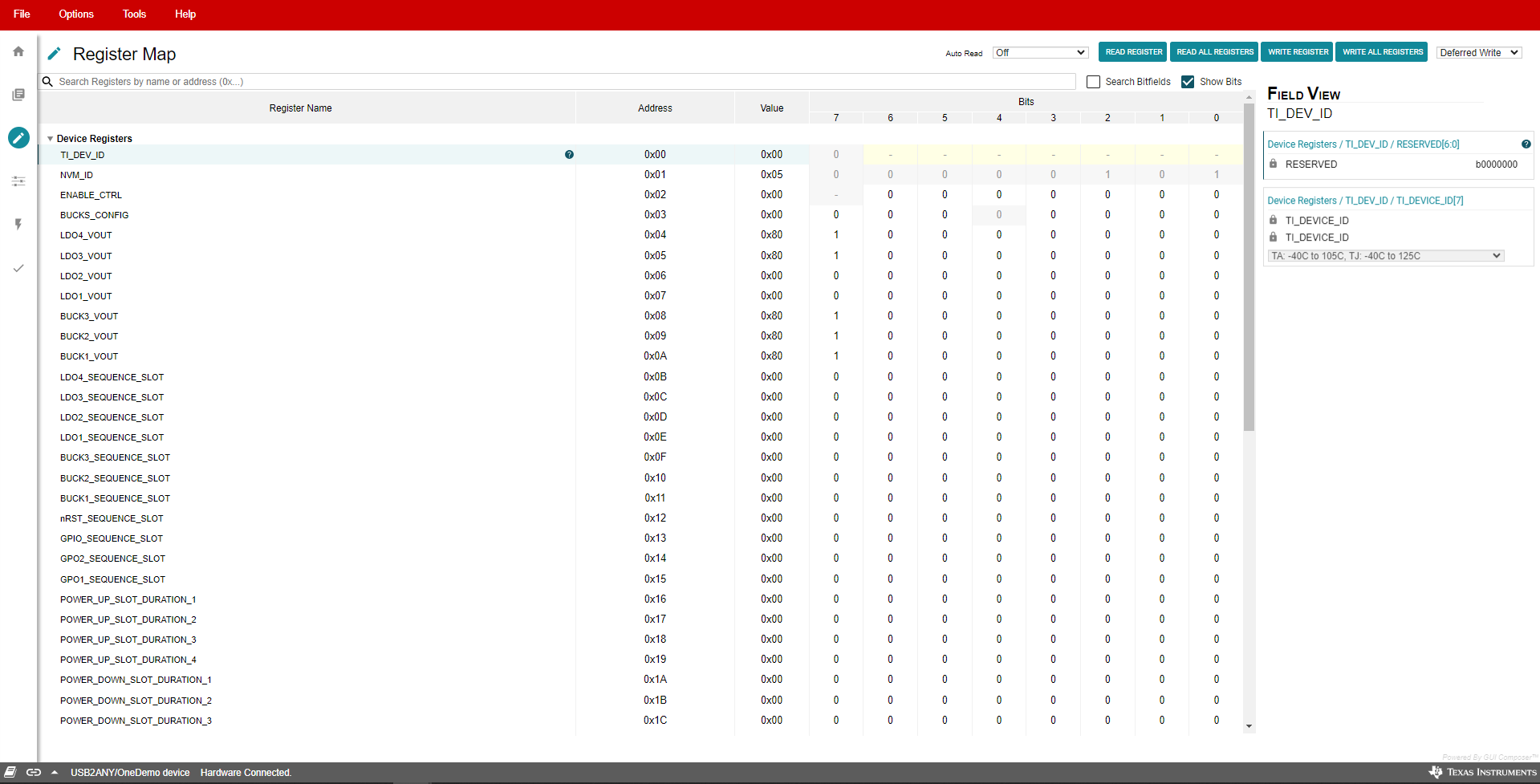
The Register Map page (shown in Figure 6-8) lists the different registers available for configuration and is intended for direct reads and writes to the PMIC registers. Reading and writing registers can be done individually or all at once. An Auto Read feature can be enabled by using the drop-down menu next to the READ ALL REGISTERS button to select an automatic read timing. Use the search bar at the top of the page to search registers by name or address.
The first three columns under the search bar show the name of each register, followed by its hexadecimal address and data value. The Bits column contains the bit values for each register and can be hidden by unchecking the Show Bits box at the top of the page, under the READ ALL REGISTERS button. Double-clicking a bit in this section changes the bit value.
The Field View section on the right side of the page shows register bits grouped by their respective control blocks. You may click on any bit field box to see the corresponding bits highlighted in yellow in the Bits column. Each field has a name shown by the blue text at the top of each box. These names can be found using the search bar by checking the Search Bitfields box (next to Show Bits).
In the Immediate Write mode (drop-down option located at the top right of the page), write buttons are greyed out since individual registers are written immediately with each change in the Field View, change in bits, or change in hexadecimal value. In Deferred Write mode, the writing of a single register or all registers is deferred until the WRITE REGISTER or WRITE ALL REGISTERS button is selected.
 Figure 6-8 Register Map Page
Although visible from the Register Map, not all registers can be edited from this page. Attempting a write to a read-only register does not generate an error. Since each write is comes with an associated read, the Register Map display is updated to reflect that the bits were not changed by the write attempt.