SLYT800B december 2020 – december 2020 LM25180 , LM25183 , LM25184 , LM5180 , LM5181
4 Small-signal Stability Review
As the waveforms in Figure 3 showed, the flyback converter delivers the entire magnetizing energy stored during the on-time (tON) to the output during the diode conduction time (tD). And unlike DCM, where the control variable is the duty cycle, a converter in BCM regulates the output voltage by varying the tON, which then controls the average diode current (ID). As a result, the duty cycle remains approximately constant, and ID—through the effective impedance of the output filter and load—establishes the output voltage.
Neglecting high-frequency phase delays related to current-mode control and PSR sample and hold, Equation 7 gives the overall loop gain as a product of the control to output (modulator and power stage), feedback, and compensator transfer functions:
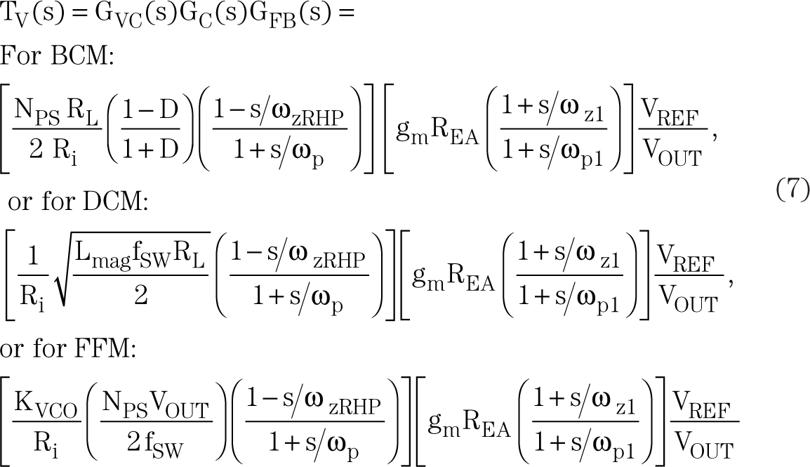
where RL is the load resistance, Ri is the effective current-sense resistance, ωp is the power-stage load pole, ωp1 and ωz1 are the pole and zero of a type-2 compensator, gmREA is the DC gain of the transconductance error amplifier, KVCO is the gain from control voltage to switching frequency in FFM, and ωzRHP is the right-half-plane zero (RHPZ) of the flyback power stage related to the phase-shift delay of the secondary current when the primary current changes. However, for DCM analysis, the RHPZ locates at sufficiently high frequency such that its effects can be ignored.
 and 42 V (Dashed Lines,
DCM)") Figure 5 PSR Flyback Converter
Waveforms at Input Voltages of 14 V (Solid Lines, BCM) and 42 V (Dashed Lines,
DCM)
Figure 5 PSR Flyback Converter
Waveforms at Input Voltages of 14 V (Solid Lines, BCM) and 42 V (Dashed Lines,
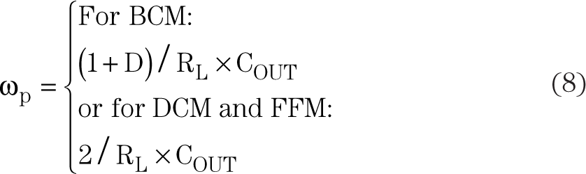
DCM)Equation 8 gives the power-stage dominant pole:
Interestingly, as the PSR sample and hold occurs at an instantaneous secondary current of zero, the left-half-plane zero evident in the control-to-output transfer function—normally associated with the output capacitor and its ESR—shows no impact on the overall loop-gain transfer function and thus is not included here. In fact, the ESR zero is offset by a corresponding pole in the feedback sampler transfer function.
Figure 6 shows Bode plot simulations of the overall loop gain for the converter circuit in Figure 1 at input voltages of 14 V and 42 V, assuming a total effective output capacitance of 22 µF. Simulation is mandatory here because practical measurements are not feasible with the integrated compensation design. Besides, the feedback node sees AC current based on the switch-voltage swing, making it unsuitable as an oscillator signal injection point for loop response measurements.
As evident from the plot in Figure 6, the frequency of the load pole is higher in DCM than BCM, and the gain of GVC(s) in DCM is generally higher. These two factors result in an increased loop gain in DCM and thus a higher crossover frequency (fC). Accordingly, the operating condition in DCM at full load sets the output capacitance requirement with reference to loop stability. If the switching frequency in DCM is 350 kHz, a good target for maximum fC is 35 kHz (10% of the switching frequency).