SLYT821 January 2022 AFE0064 , AFE1256 , AFE2256 , AFE3256 , DDC112 , DDC1128 , DDC114 , DDC118 , DDC232 , DDC264 , DDC316
3 X-ray AFE ROICs
The AFE family of readout integrated circuits (ROICs) comprises three devices: the AFE0064, AFE1256 and AFE2256.
TI originally designed AFE devices to measure the charges collected by an array of pixels (photodiodes) in a thin-film-transistor flat-panel detector. Given the nature of the signals in this application, the devices are optimized for wider input bandwidths and shorter integration times (sampling periods) well below 20 µs. Conversely, their designs are not intended for integration times longer than a few milliseconds.
The maximum charge setting (full scale) is traditionally lower than the DDC family, on the order of 10 pC. But because they target lower signals, the sensitivity/noise floor is also better than DDCs, with typical numbers around 0.1 fCrms (600 electrons). For small-charge ranges, an AFE will offer less than half the noise compared to a DDC.
The tighter dynamic range of the device (a lower noise floor but an even lower full scale) does not require the 20-plus bit converter used with DDC devices, and as such, the AFE devices support only 16-bit conversion.
Besides the increased sensitivity, one advantage is that AFE devices, unlike DDCs, can work with currents flowing either into or out of the device input without the need for external components, and even acquire bipolar signals.
The input voltage for the AFE is not zero but a different voltage level (for example, 1.68 V for the AFE0064 depending on the selected device). You must consider the voltage level when biasing the sensor. For instance, to read a photodiode while trying to keep the dark current close to zero, you would usually use a zero bias (no bias applied across the photodiode). Thus, if one terminal of the photodiode connects to the AFE input, the other terminal should be biased to the same non-zero voltage.
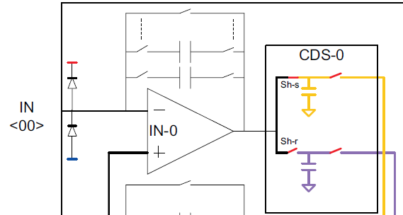
To explain the architecture of every channel further (see Figure 3-1), every sample is actually divided into two phases controlled by external signals: a reset/offset sample phase and a signal sample phase. These are the traditional phases of a correlated double sampler (CDS). In panel applications, during the reset/offset phase, the input of the device connects to the external world (usually a data line) but without the signal being present. The intention is to sample or baseline any existing offset or low-frequency noise (flicker) from external or internal sources. One-half of the CDS stores the resulting integration. In the signal sample phase, the external signal connects to the input; the other half of the CDS stores that integration. The sources of offset will still be present during this time; subtracting the two samples in the CDS will remove the offsets, leaving only the signal of interest.
 Figure 3-1 The X-ray AFE input integrator
architecture
Figure 3-1 The X-ray AFE input integrator
architectureWhen applying such a scheme to the sampling of continuous current, the reset phase will also integrate a portion of the signal that the circuit will later subtract from the integration obtained during the signal sample phase. If the signal is constant during these two phases, the effect is an easily correctable gain error. But if the signal varies, you should take the potential induced errors into account.
If it is possible to synchronize the signal generation with CDS sampling operation, there will not be a gain error. For example, if it is possible to turn sensor illumination on and off synchronous to CDS operation, the photodiode current would be generated only during the signal sample phase, not during the reset/offset phase. The result would be no gain error, with the additional advantage that any ambient light or offset would be sampled during the reset/offset phase and get rejected by the CDS.
The AFE0064 comes in a more traditional thin quad flat package (TQFP), while newer versions are available as chip-on-flex (COF) packages, driven by the flat-panel-detector application. This may present some complications versus the more common assembly methods.