SLYY200A April 2021 – December 2023 LM25149 , LM25149-Q1 , LM5156-Q1 , LM5157-Q1 , LM53635-Q1 , LM60440-Q1 , LM61460-Q1 , LM61495-Q1 , LMQ62440-Q1 , LMR33630-Q1 , LMS3655-Q1 , TPS55165-Q1 , UCC12040 , UCC12050
- 1
- Overview
- At a glance
- What is EMI?
- Conventional methods to reduce EMI in the low- and high-frequency ranges
- Innovations in reducing low-frequency emissions
- Spread spectrum
- Active EMI filtering
- Cancellation windings
- Innovations in reducing high-frequency emissions
- HotRod™ package
- Enhanced HotRod QFN
- Integrated input bypass capacitor
- True slew-rate control
- EMI modeling capabilities
- Low-frequency EMI designs using WEBENCH® design tool
- Conducted and radiated EMI results published in data sheets
- Conclusion
- Keep product categories for low EMI
HotRod™ package
One of the main approaches to reducing high-frequency emissions is to minimize the power-loop inductance. Step-down converters from TI such as the LM53635-Q1, LMS3655-Q1, LM61495-Q1, LMR33630-Q1 and LM61460-Q1 move away from bond-wire packages to leadframe-based flip-chip (HotRod) packages that help lower the power-loop inductance and in turn reduce switch-node ringing.
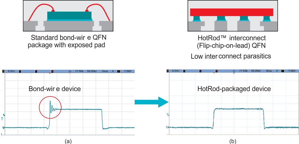
HotRod packages flip the silicon die and place it directly on a lead frame in order to minimize the parasitic inductance caused by bond-wires on pins running switching currents. Figure 17 shows the construction and benefit of HotRod packages. Along with an improvement in power-loop inductance, HotRod-style packages also help lower resistance in the power path, leading to higher efficiency while making a smaller solution size possible.
 Figure 17 Standard QFN with bond-wires
to electrically connect to the die (a); HotRod package with copper pillars and
flip-chip interconnect between the leadframe and die (b).
Figure 17 Standard QFN with bond-wires
to electrically connect to the die (a); HotRod package with copper pillars and
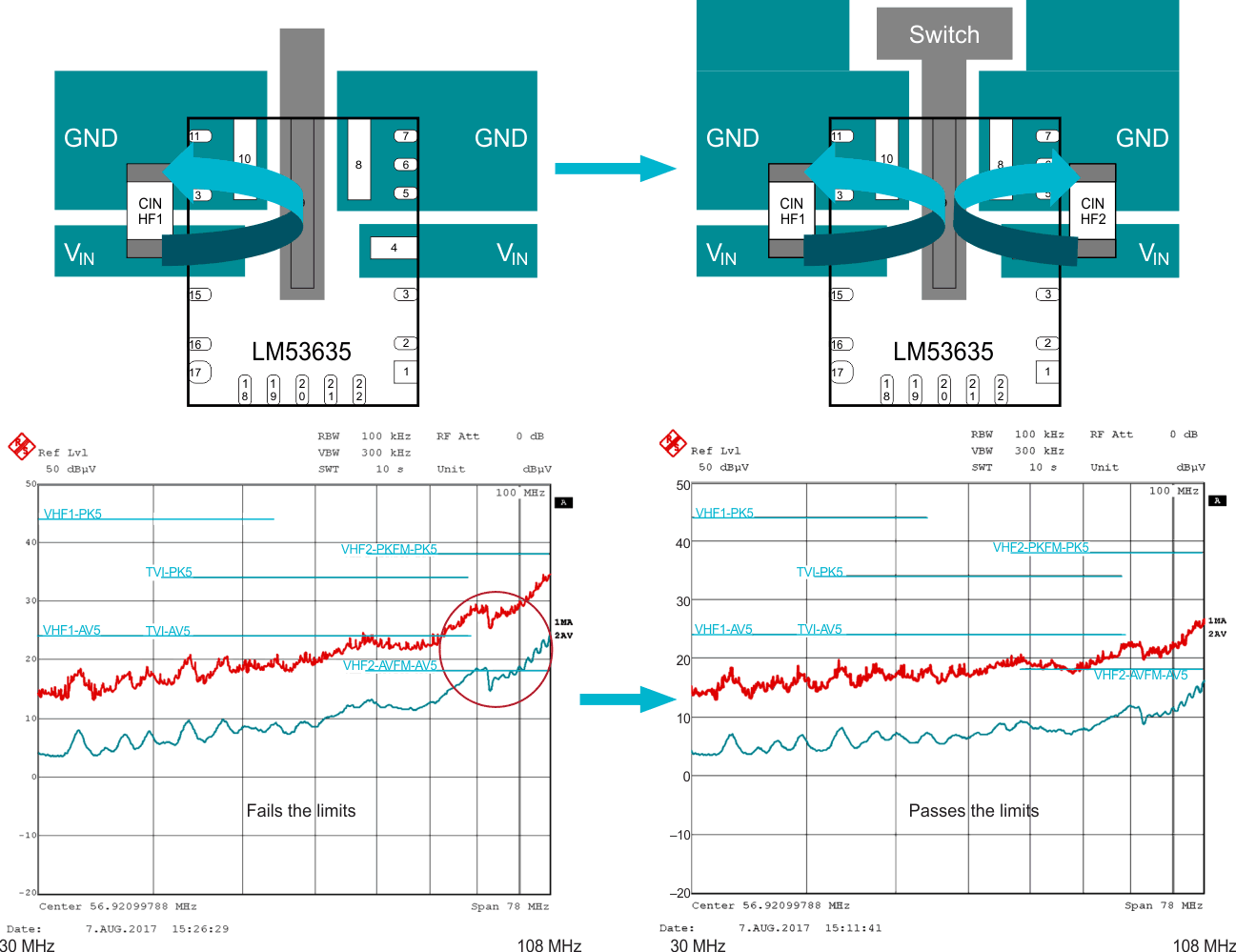
flip-chip interconnect between the leadframe and die (b).An additional benefit of devices in the HotRod package is that they facilitate parallel input path pinouts — the layout arrangement of a DC/DC converter’s input capacitors. By optimizing the pinout of the DC/DC converter so that there is symmetry in the input capacitors’ layout, the opposing magnetic fields generated by the input power loops are within the symmetric loops, thereby minimizing emissions to nearby systems. A parallel input path further minimizes high-frequency EMI, particularly in the most stringent FM band, as shown in Figure 18.
 Figure 18 Effect of the parallel input
path on EMI in an SMPS.