SNAU287 November 2023
- 1
- Description
- Features
- 4
- 1Evaluation Module Overview
- 2Hardware
- 3Software
- 4Hardware Design Files
- 5Additional Information
- 6Related Documentation
3.2.1 USB2ANY Board Connections
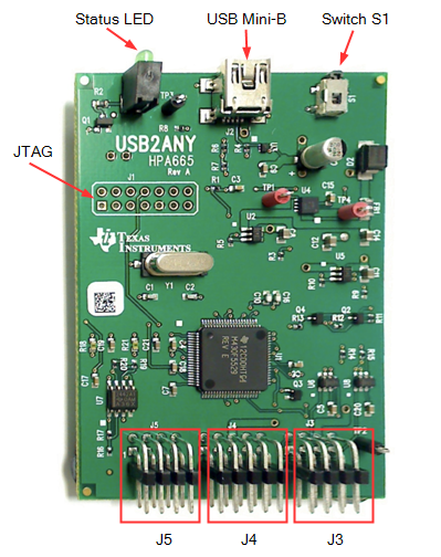
The USB2ANY has four interface connectors: one USB 2.0 connector (J2) and three I/O connectors (J3, J4, and J5). The USB connector is a standard ‘A’ type mini USB receptacle. The I/O connectors are standard dual-row, 0.1” center, pin headers.
The I/O connectors J3 and J5 are 8-pin type and J4 is a 10-pin type. The I/O connectors are configured such that the I/O connectors accept either individual cable connections or a single 30-pin connection.
 Figure 3-18 USB2ANY
Board Connections
Figure 3-18 USB2ANY
Board ConnectionsThe standard USB2ANY Kit (HPA665-001) includes both a 10-pin cable and a 30-pin cable. The 10-pin cable is intended to be connected to J4. J4 provides the SDA, SCL, and GND connections of interest.
J5 and J6 supply other connections that are NOT required and therefore, outside the scope of this document.
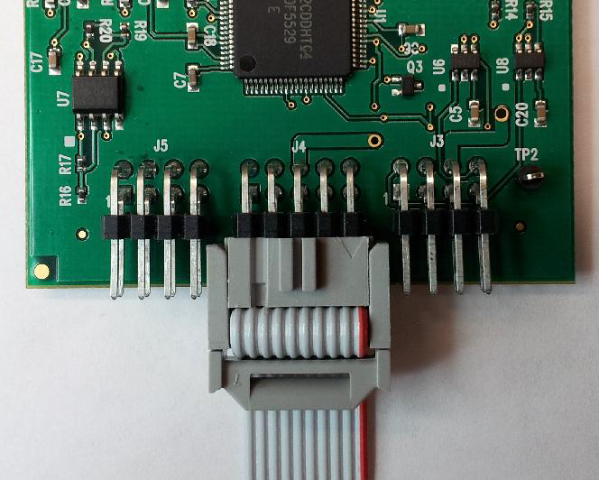
When the USB2ANY board is in the enclosure, there is a key notch above J4 that prevents the cable connector from being plugged in upside-down. With the notch at the top, pin 1 of the 10-pin cable connector is located at the upper-right corner.
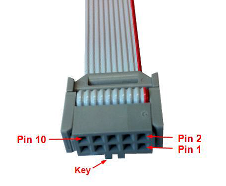
The 10-pin cable is about 6 inches in length and has a keyed female 10-pin IDC connector on each end. Figure 4-19 shows the connection of the cable to the USB2ANY board (the key must be facing up, away from the board). The opposite end of the cable must be connected to the target board. Figure 4-20 shows the indicator for pin 1, the red stripe on the cable.
 Figure 3-19 10-pin
Cable Connection to J4
 Figure 3-20 10-pin
Cable Pinout
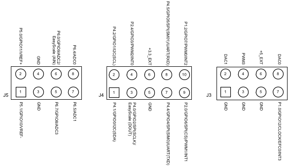
 Figure 3-21 USB2ANY
Board Connector Pinout Diagram
Figure 3-21 USB2ANY
Board Connector Pinout Diagram| Pin Name | J4 Pin # | Cable Pin # | Description |
|---|---|---|---|
| P4.1/GPIO0/I2C(SDA) | 1 | 10 | I2C Data |
| P4.2/GPIO1/I2C(SCL) | 2 | 9 | I2C Clock |
| P4.0/GPIO2/SPI(SCLK) | 3 | 8 | General-purpose digital I/O (not required) |
| P2.4/GPIO3 | 4 | 7 | General-purpose digital I/O (not required) |
| GND | 5 | 6 | Common Ground |
| +3.3_EXT | 6 | 5 | +3.3V output power supply (100 mA limit) |
| P4.4/GPIO4/SPI(SIM0) | 7 | 4 | General-purpose digital I/O (not required) |
| P4.5/GPIO5/SPI(SM01) | 8 | 3 | General-purpose digital I/O (not required) |
| P2.0/GPIO6/SPI(CS) | 9 | 2 | General-purpose digital I/O (not required) |
| P1.2/GPIO7 | 10 | 1 | General-purpose digital I/O (not required) |
Instead of using the 10-pin header and supplied cable, a board designer can alternatively choose to use a 3-pin I2C header on the application board and 3 jumper wires to connect the SDA, SCL, and GND signals from J4 of USB2ANY to the I2C header.