SNAU299 January   2024 LMX1214


  1.   1
  2.   Description
  3.   Features
  4.   Applications
  5.   5
  6. 1Evaluation Module Overview
    1. 1.1 Introduction
    2. 1.2 Kit Contents
    3. 1.3 Specification
    4. 1.4 Device Information
  7. 2Hardware
    1. 2.1  Evaluation Setup Requirement
    2. 2.2  Connection Diagram
    3. 2.3  Power Requirements
    4. 2.4  How to Enable Full SPI Control
    5. 2.5  Reference Clock
    6. 2.6  Output Connections
    7. 2.7  Switch Information
    8. 2.8  Default Configuration
    9. 2.9  Divider Mode Example
    10. 2.10 Hybrid Mode: SPI and Pin Mode
  8. 3Software
    1. 3.1 Software Installation
    2. 3.2 Software Description
    3. 3.3 USB2ANY Interface
  9. 4Implementation Results
    1. 4.1 Evaluation Setup
      1. 4.1.1 Buffer and Divider Mode
  10. 5Hardware Design Files
    1. 5.1 Schematic
    2. 5.2 PCB Layout
      1. 5.2.1 PCB Layer Stack-Up
    3. 5.3 Bill of Materials
  11. 6Additional Information
    1. 6.1 Troubleshooting Guide
      1. 6.1.1 General Guidance
      2. 6.1.2 If Output Is Not Seen on CLKOUT
      3. 6.1.3 If Device Features Are Not Active
      4. 6.1.4 If Divider Frequency Is Not Accurate
    2. 6.2 Trademarks

Schematic

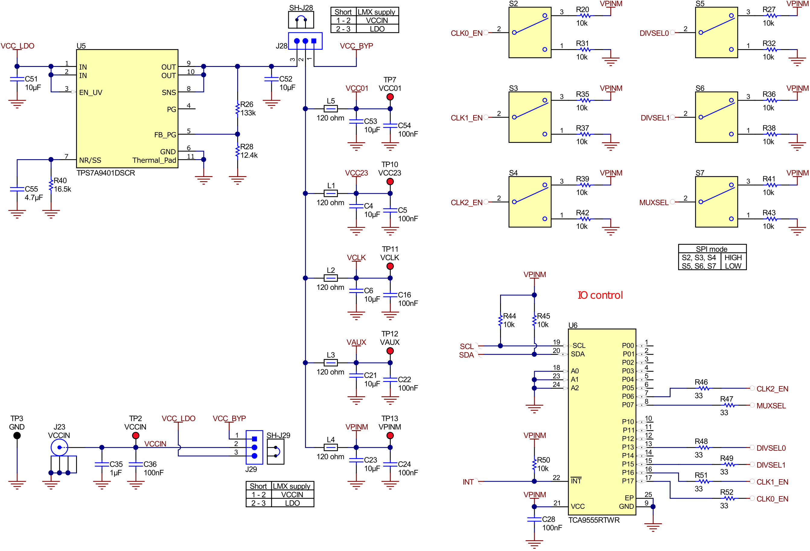
GUID-20240130-SS0I-P96G-6XL8-GTX9NBVRVD2M-low.png Figure 5-1 Power Supply, IO Control, Switches
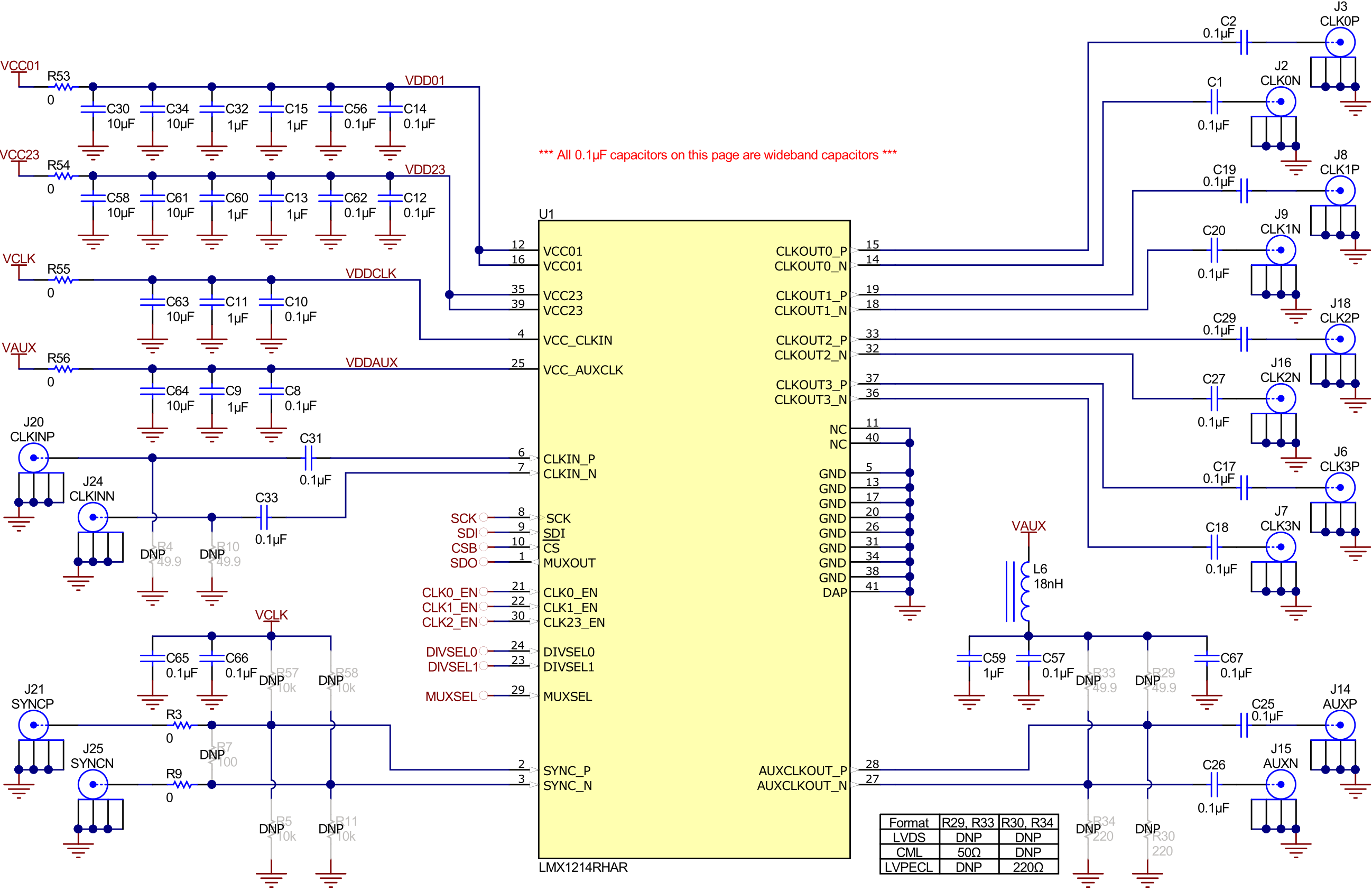
GUID-20240130-SS0I-L7B6-HXSM-QQKPSBHTW4BD-low.png Figure 5-2 LMX1214
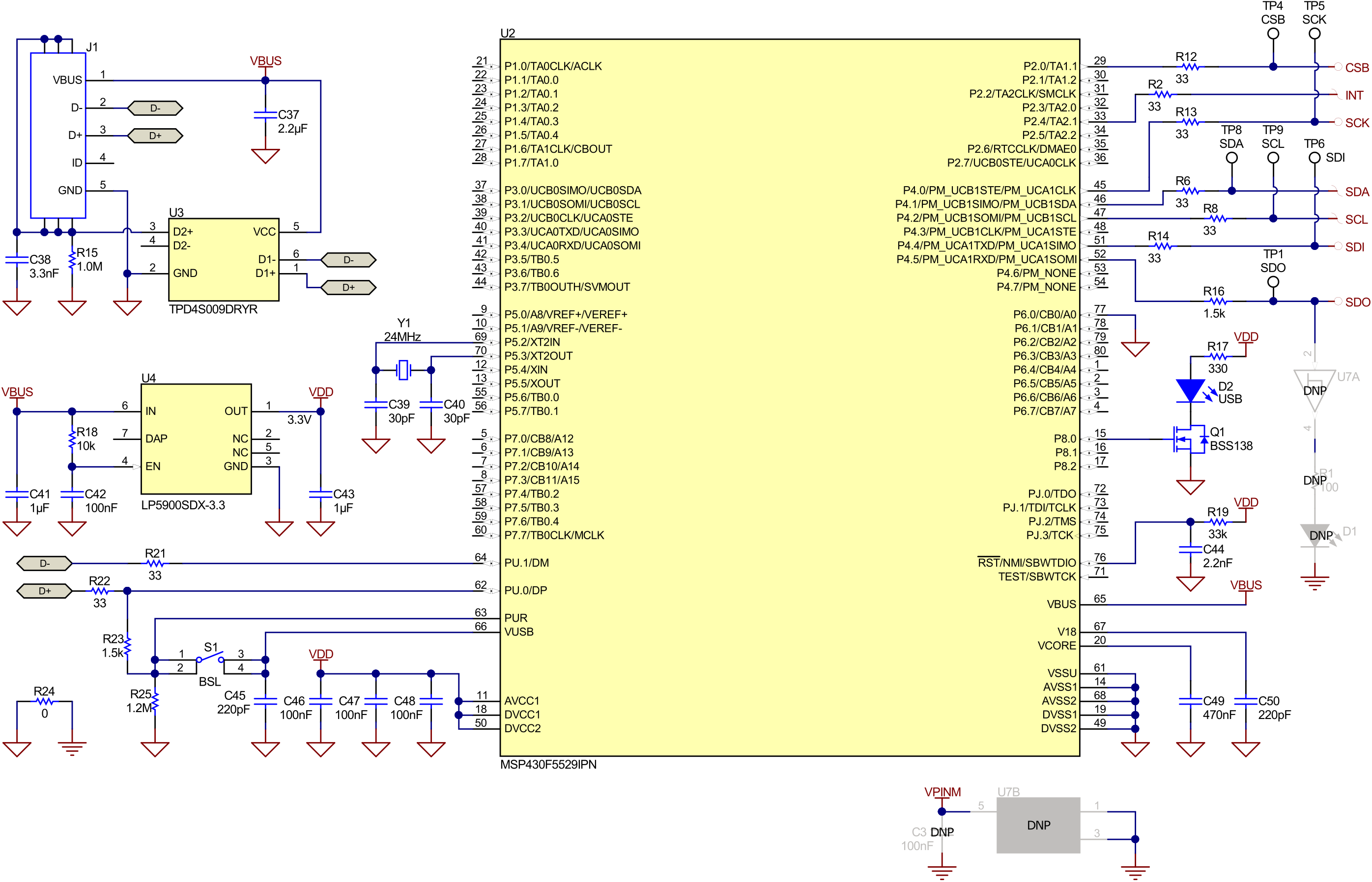
GUID-20240130-SS0I-DPQX-WBP6-PMMQTVFVZGCS-low.png Figure 5-3 USB2ANY Interface