SNLA353 August 2020 DS90LV011A
4 Devices With Termination Resistors
- The following scenario is used when the device that is being used for the receiver already contains a termination resistor. The process and the equations are roughly the same with just a few adjustments due to the added resistance. Ensure that the receiver being used contains a termination resistor and obtains the value of the resistance from the data sheet.
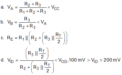
- If your device does contains internal termination, then the equations shown in Figure 4-1 will be used.
 Figure 4-1 Equations for a Receiver With Internal
Termination
Figure 4-1 Equations for a Receiver With Internal
Termination- For the simulation, the following values
will be used:
- VCC = 3.3 V
- VA = 1.2 V, LVDS driver output fixed common mode voltage
- VB = 0.9 V, Sub-LVDS driver output fixed common mode voltage
- RE = 50Ω
- RT = 100Ω, value of termination resistor inside device
- Using the formulas a, b, and c from Section 2 creates a system of
equations in order to solve for the resistance values that will best fit the desired
parameters for Sub-LVDS. The following values were obtained from the system of equations:
- R1 = 222Ω
- R2 = 32Ω
- R3 = 95Ω
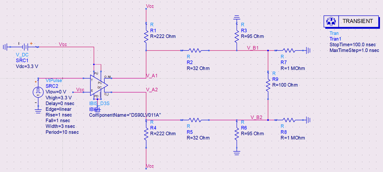
Proceed to simulate the circuit in order to verify the correct behavior.
 Figure 4-2 Schematic for Receivers With Internal
Termination
Figure 4-2 Schematic for Receivers With Internal
TerminationNote: Resistors R7 and R8
are used to imitate the high impedance inputs of a receiver.
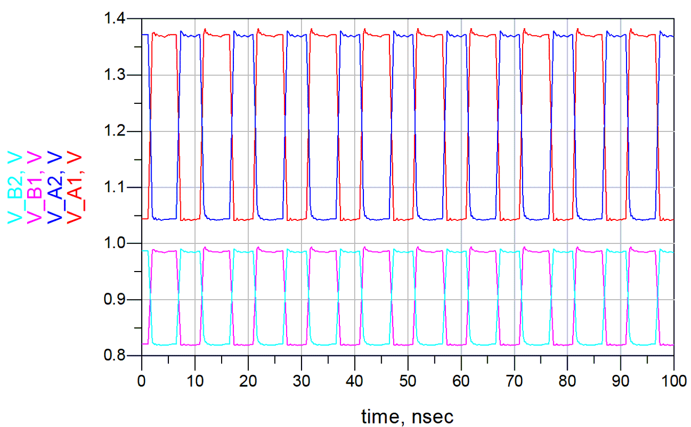
- The simulation shown in Figure 4-3 demonstrates a voltage swing of approximately:
- VID ≈ 160 mV
- VOD ≈ 325 mV
- VID falls within the desired
range. If the formulas are used to obtain values for VID, VCMF, and
RE with the resistor values and the measured values for VOD and
VA then we obtain the following results:
- VID = 163 mV
- VB = 0.9 V
- RE = 50Ω
 Figure 4-3 Simulation Results for Devices With
Internal Termination