SNLA437 December 2023 DP83822H , DP83822HF , DP83822I , DP83822IF , DP83825I , DP83826E , DP83826I
- 1
- Abstract
- Trademarks
- 1DP83822 Application Overview
-
2Troubleshooting the PHY Application
- 2.1 Schematic and Layout Checklist
- 2.2 Verify Successful Power-up of PHY
- 2.3 Read and Check Register Values
- 2.4 Peripheral Pin Checks
- 2.5 Verifying Strap Configurations During Initialization
- 2.6 Debugging Link Quality
- 2.7 Built-In Self Test With Various Loopback Modes
- 2.8 Debug the Fiber Connection
- 2.9 Debug the MAC Interface
- 2.10 Debug the Start of Frame Detect
- 2.11 Tools and References
- 3References
2.9 Debug the MAC Interface
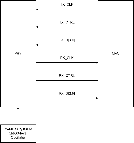
RGMII
The RGMII signals are summarized in Table 2-10.
| Function | Pins |
|---|---|
| Data Signals | TX_D[3:0] |
| RX_D[3:0] | |
|
Transmit and Receive Signals |
TX_CTRL |
| RX_CTRL | |
| Clock | TX_CLK |
| RX_CLK |
 Figure 2-12 RGMII Signaling
In order for the MAC to be able to transmit and receive the correct data from the PHY, the correct RGMII modes must be selected such that both the PHY and the MAC are not simultaneously in align mode or shift mode for the Tx and Rx side. Table 2-11 lists the correct RGMII delay configurations.
| MAC Configuration | Required PHY Configuration |
|---|---|
| RGMII Align on Rx | RGMII Shift on Rx |
| RGMII Shift on Rx | RGMII Align on Rx |
| RGMII Align on Tx | RGMII Shift on Tx |
| RGMII Shift on Tx | RGMII Align on Tx |
Reference the waveforms below to verify the expected MAC data and clock signals for RGMII Mode. The table displays specs taken from the device-specific data sheet that are shown in the waveforms.
 Figure 2-13 RX_CLK and RX_D0 Timing in
RGMII Align Mode (Yellow Waveform (Channel 1) = RX_CLK, Blue Waveform (Channel
2) = RX_D0)
 Figure 2-14 RX_CLK and RX_D0 Timing in
RGMII RX Shift Mode (Yellow Waveform (Channel 1) = RX_CLK, Blue Waveform
(Channel 2) = RX_D0)
Figure 2-14 RX_CLK and RX_D0 Timing in
RGMII RX Shift Mode (Yellow Waveform (Channel 1) = RX_CLK, Blue Waveform
(Channel 2) = RX_D0)For RGMII Rx shift mode, verify that RX_CLK is shifted by 3.5 ns and for RGMII TX Clock Shift that TX_CLK is shifted by 3.5 ns.
| Parameter | Test Condition | Min | Typ | Max | Unit |
|---|---|---|---|---|---|
| Tcyc | TX_CLK / Clock Cycle Duration | 36 | 40 | 44 | ns |
| Tsetup(align) | TX_D[3:0], TX_CTRL setup to TX_CLK (align mode) | 1 | 2 | ns | |
| Thold(align) | TX_D[3:0], TX_CTRL hold to TX_CLK (align mode) | 1 | 2 | ns |
| Parameter | Test Condition | Min | Typ | Max | Unit |
|---|---|---|---|---|---|
| Tskew(align) |
RX_D[3:0], RX_CTRL delay from RX_CLK (align mode) |
-500 |
0 |
ps | |
| Tsetup(shift) | RX_D[3:0], RX_CTRL delay from RX_CLK (shift mode enabled, default) | 1.2 | 2 | ns | |
| Tcyc | RX_CLK / Clock Cycle Duration | 36 | 40 | 44 | ns |
| Duty_G | RX_CLK / Duty Cycle | 40 | 50 | 60 | % |
| Tr/Tf | RX_CLK / Rise, Fall Time (20% to 80% ) | 750 | ps |
RMII
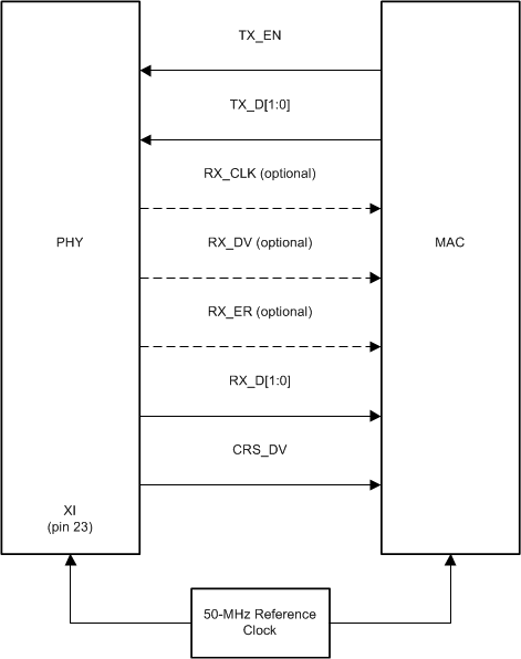
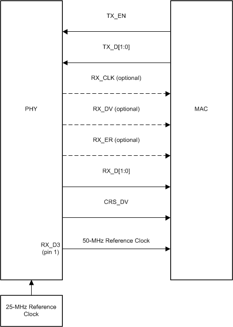
The incorporates the Reduced Media Independent Interface (RMII) as specified in the RMII specification from the RMII consortium. The purpose of this interface is to provide a reduced pin count alternative to the IEEE 802.3u MII as specified in Clause 22. Architecturally, the RMII specification provides an additional reconciliation layer on either side of the MII, but can be implemented in the absence of an MII. The offers two types of RMII operations: RMII Slave and RMII Master. In RMII Slave operation, the operates off of a 50-MHz CMOS-level oscillator connected to the XI pin and shares the same clock as the MAC. In RMII Master operation, the operates off of either a 25-MHz CMOS-level oscillator connected to XI pin or a 25-MHz crystal connected across XI and XO pins. A 50-MHz output clock referenced from any of the three GPIOs is connected to the MAC.
The RMII specification has the following characteristics:
- Supports 100BASE-FX, 100BASE-TX and 10BASE-Te.
- Single clock reference sourced from the MAC to PHY (or from an external source)
- Provides independent 2-bit wide transmit and receive data paths
- Uses CMOS signal levels, the same levels as the MII interface
In this mode, data transfers are two bits for every clock cycle using the internal 50-MHz reference clock for both transmit and receive paths.
The RMII signals are summarized in Table 2-14.
| Function | Pins |
|---|---|
| Data Signals | TX_D[1:0] |
| RX_D[1:0] | |
| Transmit and Receive Signals | TX_EN |
| CRS_DV |
 Figure 2-15 RMII Slave Signaling
 Figure 2-16 RMII Master Signaling
For more information on reduced media independent interface, see the Reduced Media Independent Interface (RMII) section of the DP83822 Robust, Low Power 10/100 Mbps Ethernet Physical Layer Transceiver Data Sheet.
 Figure 2-17 RX_CLK and RX_D0 Timing for
RMII (Yellow Waveform (Channel 1) = RX_CLK, Blue Waveform (Channel 2) =
RX_D0)
Figure 2-17 RX_CLK and RX_D0 Timing for
RMII (Yellow Waveform (Channel 1) = RX_CLK, Blue Waveform (Channel 2) =
RX_D0)MII
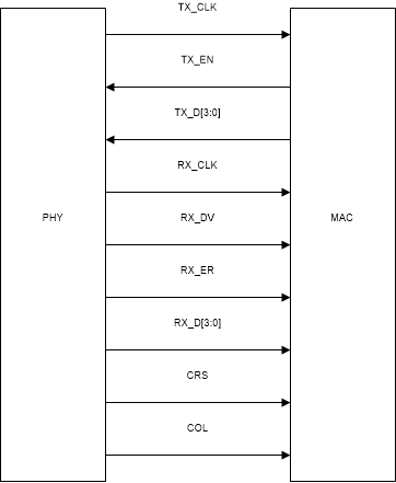
The Media Independent Interface is a synchronous 4-bit wide nibble data interface that connects the PHY to the MAC . The MII is fully compliant with IEEE 802.3-2002 clause 22.
The MII signals are summarized in Table 2-15.
| Function | Pins |
|---|---|
| Data Signals | TX_D[3:0] |
| RX_D[3:0] | |
| Transmit and Receive Signals | TX_EN |
| RX_DV | |
| Line-Status Signals | CRS |
| COL | |
| Clock | TX_CLK |
| RX_CLK |
 Figure 2-18 MII Signaling
Additionally, the MII interface includes the carrier sense signal (CRS), as well as a collision detect signal (COL). The CRS signal asserts to indicate the reception or transmission of data. The COL signal asserts as an indication of a collision which can occur during Half-Duplex mode when both transmit and receive operations occur simultaneously.
 Figure 2-19 RX_CLK and RX_D0 Timing for MII (Blue Wave (Channel 2) = RX_CLK,
Purple Wave (Channel 3) = RX_D0)