SNLU237A September 2018 – January 2024 DP83869HM
- 1
- DP83869EVM
- Trademarks
- 1Definitions
- 2Introduction
- 3Board Setup Details
-
4Configuration Options
- 4.1
Bootstrap Options
- 4.1.1 Straps for PHY Address
- 4.1.2 Strap for DP83869 Functional Mode Selection
- 4.1.3 Straps for RGMII/SGMII to Copper
- 4.1.4 Straps for RGMII to 1000Base-X
- 4.1.5 Straps for RGMII to 100Base-FX
- 4.1.6 Straps for Bridge Mode (SGMII-RGMII)
- 4.1.7 Straps for 100 M Media Converter
- 4.1.8 Straps for 1000 M Media Convertor
- 4.2 SGMII/Fiber Interface
- 4.3 RGMII
- 4.4 Clock Output
- 4.5 Clock Input
- 4.6 Switch Configuration Options
- 4.1
Bootstrap Options
- 5Schematics
- 6Revision History
2.2.2 External Power Supply Operation
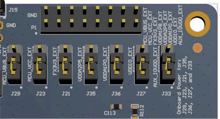
 Figure 2-4 Jumper Placements for Onboard Power
The jumpers shown in Figure 2-4 can be used to choose whether a particular voltage rail is supplied through onboard LDOs or an external power supply. If an external power supply is desired on a voltage rail, then change the respective jumper from position 1-2 (LDO) to 2-3 (External). Then, connect the appropriate voltage on the corresponding pin to the P1 connector. For example, if the VDDA2P5 is to be supplied from an external supply, then change jumper position of J35 from 1-2 to 2-3. Then connect the 2.5-V external supply on pins 9-10 on the P1 connector. Note that pin 9 is supply and pin 10 is ground.