SNOAA68 June 2021 LMG3410R050 , LMG3410R070 , LMG3410R150 , LMG3411R050 , LMG3411R070 , LMG3411R150 , LMG3422R030 , LMG3422R050 , LMG3425R030 , LMG3425R050 , LMG3522R030-Q1 , LMG3526R030
7 Achieving Surge Robustness
The association of avalanche rating with surge robustness arises because the drain breakdown voltage of Si power FETs is typically limited by impact ionization or avalanche breakdown. When a power-line surge strikes, the FET breaks down by avalanche as its drain voltage exceeds the breakdown voltage. Silicon FETs therefore provide surge robustness via avalanche capability.
GaN has much lower impact ionization coefficients than Si(21, 22) as a result of its superior high-field withstand properties. The voltage rating of GaN FETs is not limited by avalanche, and there is headroom above it for transient events. As a result, GaN FETs have the ability to switch through surge events. GaN FETs are surge robust because they have transient overvoltage capability.
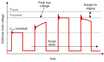
The data sheet parameter, VDS(SURGE), was introduced to quantify the peak bus voltage that may be applied to the GaN FET when actively switching the load current during a surge strike(23, 24). This definition provides a simple specification for surge-robust power supply design. VDS(SURGE) supplements the VDS(TR) rating already present in the data sheets of several manufacturers. VDS(TR) is typically measured with the device off, and therefore quantifies the margin available for ringing (for example, with the channel off). Figure 7-1 shows these parameters.
 Figure 7-1 VDS(SURGE) is the
peak bus voltage the GaN FET can actively switch through during surge.
VDS(TR) provides extra margin for ringing.
Figure 7-1 VDS(SURGE) is the
peak bus voltage the GaN FET can actively switch through during surge.
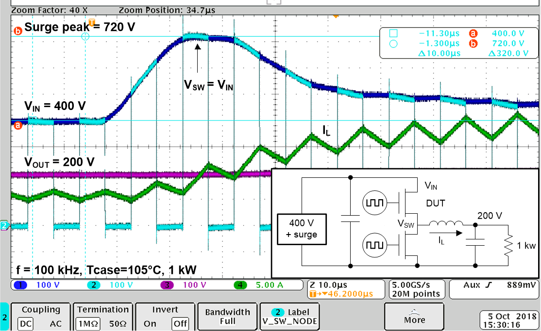
VDS(TR) provides extra margin for ringing.TI GaN FETs are validated for VDS(SURGE) by applying fifty strikes per the IEC 61000-4-5 surge standard(25) to a half-bridge delivering power under actual use hard-switching conditions. A detailed description of the validation of the LMG3410R070 is provided in reference 24. Fifty strikes per VDE 0884-11(26) were applied to a half bridge operating at VDS = 400 V, 100 kHz, 50% duty cycle, and delivering 1 kW of power with a case temperature of the hard-switching device at 105°C. The peak bus voltage at the devices was set to 720 V. The schematic and waveforms are shown in Figure 7-2. The figure shows the bus voltage surging to 720 V with application of the strike. The switched node waveform is overlaid on the input waveform to show the switching transitions. An increase in the inductor current from 5 A to 20 A is also seen, further validating the robustness. The use of a half-bridge allows the validation of all modes of device operation under both voltage and current surges: hard switching, soft switching, blocking, and third quadrant operation and its hard-commutation turn-off. The test does not cause hard-fail or efficiency degradation.

Figure 7-2 Surge waveforms, showing the test point parameters of the schematic (inset). The switched node waveform is overlaid on the input waveform to show switching through the surge strike.
The surge-voltage specification, VDS(SURGE), makes it straightforward to design a robust power supply with GaN. This is because the schematic for a surge generator is specified in the standard and can be implemented in a simulator. This allows component values to be selected such that the bus voltage at the device remains below 720 V during surge. Our simulations showed that the application of a 4-kV surge strike to the input of a power supply resulted in a peak bus voltage of only 570 V at the GaN FET. Four kV is the highest defined voltage of the IEC surge standard. This shows that it is straightforward to limit the peak surge voltage at the FET with margin, even for severe surge conditions.
The overvoltage capability of GaN is advantageous to the avalanche capability of Si. It allows the power supply to not drop the load and provide a robust power solution. Overvoltage ability also provides more protection margin than avalanche over the system lifetime. This is because FETs do not have the avalanche capability to absorb much energy or offer much clamping, therefore the clamping circuitry needs to bear the brunt of the surge. Degradation of the clamping circuitry, for example, MOVs over their lifetime will expose an avalanching FET to higher levels of surge voltage and increase the risk of failure.