SNVA115B May 2005 – February 2022 LM3475
3 Optional Components
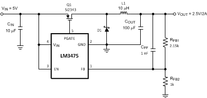
A feedforward capacitor, CFF, is placed on the board, which will increase operating frequency. However, the speed up effect decreases with lower output voltage and is negligible below 1.6-V output.
A 0 Ω is used to pull up the EN pin for always on operation. The enable pin can be pulled low at the EN post to shutdown the device. If this resistor is removed, any analog level signal can be used to enable and disable the device.
 Figure 3-1 Full Demo Board
Schematic
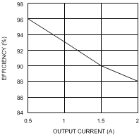
 Figure 3-2 Efficiency vs Output Current
(VIN = 5 V)
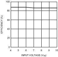
 Figure 3-3 Efficiency vs Input Voltage
(Iout = 2 A)
Figure 3-3 Efficiency vs Input Voltage
(Iout = 2 A)Table 3-1 Bill of Materials
(BOM)
| Designator | Part Description | Part Number |
|---|---|---|
| CIN | 10 µF, 16-V ceramic | Yuden EMK325BJ106MN |
| COUT | 100 µF, 6-V tantalum | AVX TPSY107M006R0100 |
| CFF | 1 nF, 25-V ceramic | VJ1206Y102KXXA |
| D1 | Schottky 20 V, 2 A | Central CMSH2-20L |
| L1 | 10 µH, 3.1 A | Sumida CDRH103R100 |
| Q1 | Si 2343 30 V, 2.5 A | Vishay Si2343 |
| RFB2 | 1 kΩ | Vishay CRCW08051001F |
| RFB1 | 2.15 kΩ | Vishay CRCW08052151F |
| R2 | 0 Ω | Vishay CRCW08050R00F |