SNVA966 July 2020 – MONTH LP8864-Q1 , LP8864S-Q1 , LP8866-Q1 , LP8866S-Q1
- Trademarks
- 1Fault Handling Routine
- 2Different Fault and Diagnostic Handling Method Recommendation
- 3Summary
-
A Fault-Related
Functions
-
A.1 Protection and Fault Detections
- A.1.1 Supply Faults
-
A.1.2 Boost Faults
- A.1.2.1 Boost Overvoltage Faults (BSTOVPL, BSTOVPH)
- A.1.2.2 Boost Overcurrent Faults (BSTOCP)
- A.1.2.3 LEDSET Resistor Missing Faults (LEDSET)
- A.1.2.4 MODE Resistor Missing Faults (MODESEL)
- A.1.2.5 FSET Resistor Missing Faults (FSET)
- A.1.2.6 ISET Resistor Out of Range Faults (ISET)
- A.1.2.7 Thermal Shutdown Faults (TSD)
- A.1.3 LED Faults
- A.1.4 Overview of the Fault and Protection Schemes
- A.2 Programming Examples
-
A.1 Protection and Fault Detections
A.1.1.1 VIN Undervoltage Faults (VINUVLO)
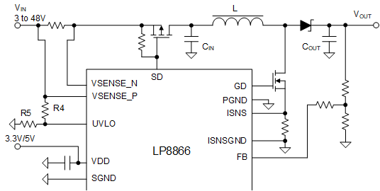
The LP886XX-Q1 device supports VIN undervoltage and overvoltage protection. The undervoltage threshold is programmable through external resistor divider on UVLO pin. If during operation of the LP886XX-Q1 device, the UVLO pin voltage falls below the UVLO falling level (0.787 V typical), the boost, LED outputs, and power-line FET will be turned off, and the device will enter STANDBY mode. The VINUVLO_STATUS bit is also set in the SUPPLY_FAULT_STATUS register, and the INT pin is triggered. When the UVLO voltage rises above the rising threshold level the LP886XX-Q1 exits STANDBY and begins the start-up sequence.
 Figure 4-1 VIN UVLO Setting Circuit