SNVAA31 November 2021 LM61435-Q1 , LM61440-Q1 , LM61460-Q1 , LM62435-Q1 , LM62440-Q1
2.3 Component Selection Connection Instructions
Below is a list of considerations when using the LM614xx and LM624xx in the universal PCB layout design. Using the LM61460EVM as the basis for the universal PCB layout, only three additional components (C10, C13, and R4) are required to enable an easy swap between the LM614xx and LM624xx (Refer to Figure 2-1 for modified EVM schematic and Figure 2-2 for 3D EVM view of additional components).
Additional Components:
- R4 is the MODE_H pull up resistor for FPWM operation with the LM624xx
- C10 and C13 are the AC coupling capacitors for external synchronization on the SYNC pin of the LM614xx and LM624xx
LM614xx Component Selection Instructions:
- Pin 6 is RT pin on this device. Populate resistor RT/MODEL_L for desired switching frequency and leave resistor MODE_H resistor as DNP.
- Pin 7 is EN/SYNC. For external synchronization, populate (LM614xx)_CSYNC capacitor and leave capacitor (LM624xx)_CSYNC as DNP. Applying a valid external switching frequency on TP4 will set the device to FPWM Mode.
LM624xx Component Selection Instructions:
- Pin 6 is MODE/SYNC on this device.
- For Auto Mode feature, populate resistor RT/MODE_L and leave resistor MODE_H as DNP.
- For FPWM Mode feature, populate resistor MODE_H and leave resistor RT/MODE_L as DNP.
- For external synchronization, populate (LM624xx)_CSYNC capacitor and leave capacitor (LM614xx)_CSYNC as DNP. Applying a valid external switching frequency on TP4 will set the device to FPWM Mode.
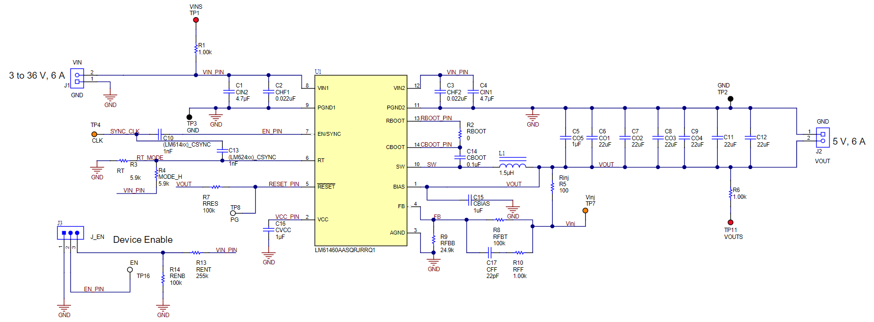 Figure 2-1 Universal Schematic with the
LM61460-Q1
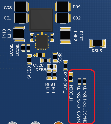 Figure 2-2 Universal PCB Layout 3D
View
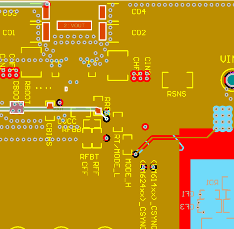 Figure 2-4 Universal PCB Layout Mid
Layer 1
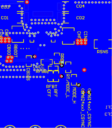 Figure 2-6 Universal PCB Layout
Bottom Layer
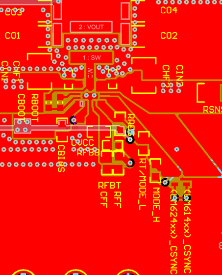 Figure 2-3 Universal PCB Layout Top
Layer
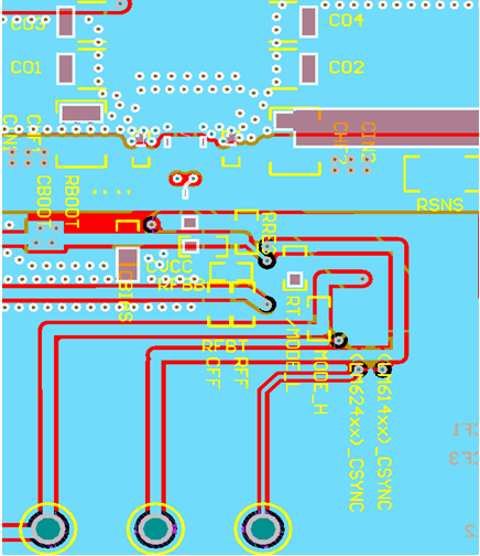 Figure 2-5 Universal PCB Layout Mid
Layer 2