SNVU869 august   2023 LM5185-Q1


  1.   1
  2.   Description
  3.   Get Started
  4.   Features
  5.   Applications
  6.   6
  7. 1Evaluation Module Overview
    1. 1.1 Introduction
    2. 1.2 Kit Contents
    3. 1.3 Specification
    4. 1.4 Device Information
  8. 2Hardware
    1. 2.1 Setup
    2. 2.2 Header Information
    3. 2.3 Test Points
    4. 2.4 Assembly Instructions
    5. 2.5 Best Practices
  9. 3Implementation Results
    1. 3.1 Performance Data and Results
      1. 3.1.1 Conversion Efficiency
      2. 3.1.2 Output Voltage Regulation
      3. 3.1.3 Operating Waveforms
        1. 3.1.3.1 Start-up
        2. 3.1.3.2 Load Transient Response
        3. 3.1.3.3 Switching
    2. 3.2 Thermal Performance
  10. 4Hardware Design Files
    1. 4.1 Schematic
    2. 4.2 PCB Layout
    3. 4.3 Bill of Materials (BOM)
  11. 5Compliance Information
    1. 5.1 Compliance and Certifications
  12. 6Additional Information
    1. 6.1 Trademarks

Switching

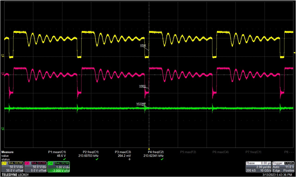
GUID-20230713-SS0I-BNS2-QKMC-43HLHKC0BTZS-low.png
C1=SW; C2=Vsec; C4=Vcomp
Figure 3-6 FFM Operation: VIN=48 V, Iout= 0.1A
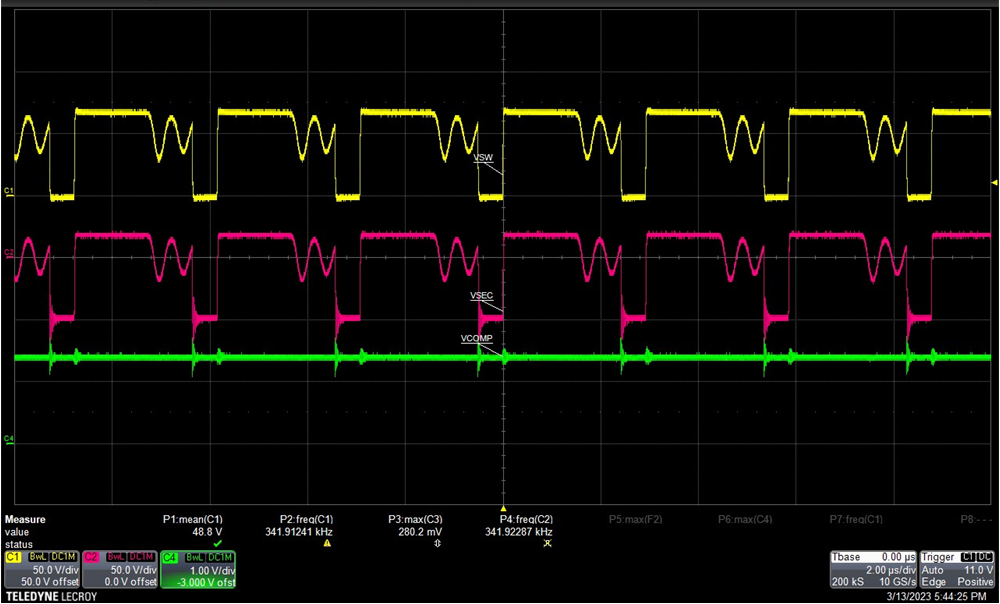
GUID-20230713-SS0I-6WZD-LXG9-DTFWGS3277X1-low.png
C1=SW; C2=Vsec; C4=Vcomp
Figure 3-7 DCM Operation: Vin=48V, Iout=0.5A
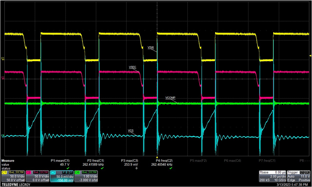
GUID-20230713-SS0I-9ZNG-8KTQ-LWDSBJ7PDJKV-low.png Figure 3-8 BCM Operation: Vin=48V, Iout=1.0A