SPRAAV1C May 2009 – March 2020 AM3703 , AM3715 , OMAP3503 , OMAP3515 , OMAP3525 , OMAP3530
-
PCB Design Guidelines for 0.4mm Package-On-Package (PoP) Packages, Part I
- Trademarks
- 1 Using This Guide
- 2 A Word of Caution
- 3 A Team Sport
- 4 Be Wary of Quotes
- 5 Don’t Forget Your CAD Tools
- 6 Metric Vs English
- 7 PCB Fab Limits
- 8 Routing and Layer Stackup
- 9 OMAP35x 0.4mm Pitch
- 10 Pad Type
- 11 PCB Pad Dimensions for 0.4mm BGA Package
- 12 Multiple BGA Packages
- 13 Etch Traps and Heat Sinks
- 14 Vias and VIP
- 15 Laser Blind Vias
- 16 Filled Vias
- 17 Know Your Tools
- 18 BeagleBoard
- 19 BeagleBoard Views
- 20 OMAP35x Decoupling
- 21 PCB Finishes for High Density Interconnect (HDI)
- 22 Real World Second Opinion
- 23 Acknowledgments
- 24 References
- Revision History
20 OMAP35x Decoupling
There are a lot of power pins on the OMAP35x. Decoupling capacitors are required and must be placed as close to the ball connection as possible. When selecting a power and ground, choose the ground closest to the power pin for each decoupling capacitor. A single decoupling capacitor can serve up to three balls.
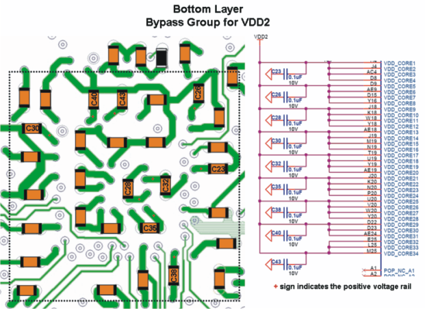
The BeagleBoard has almost all of its decoupling capacitors mounted on the bottom side of the board. Each capacitor connects with as many as three processor power pins through both blind vias to the power plane and thru-hole vias from top to bottom.
Figure 25 shows how the OMAP335xx’s VDD2 rail is decoupled on the BeagleBoard. The processor outline is shown as a dotted line and the PCB design is viewed from the top side. The schematic for this area is shown to the right and the reference designators are shown on the appropriate capacitors.
The bypass capacitors are 0.1μF, 10 V, X7R type and are in a 0402 package.
There are additional voltage rails that use the remaining capacitors. A careful study of the BeagleBoard Gerbers and schematics will help you as your design is realized and illustrate what worked for this board.
 Figure 25. BeagleBoard Bypass Group for VDD2