SPRABJ8B September 2022 – November 2023 AM2631 , AM2631-Q1 , AM2632 , AM2632-Q1 , AM2634 , AM2634-Q1 , AM263P4 , AM263P4-Q1
5.2 OSPI/QSPI Memory Implementation
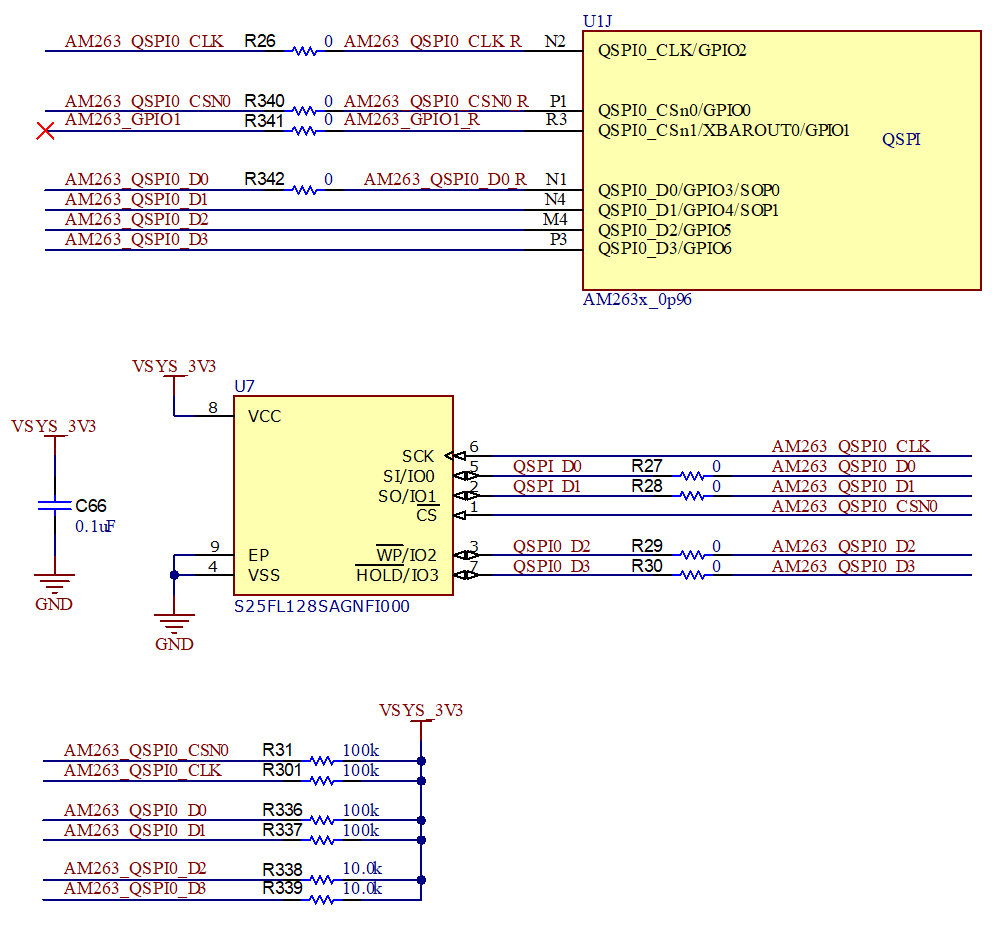
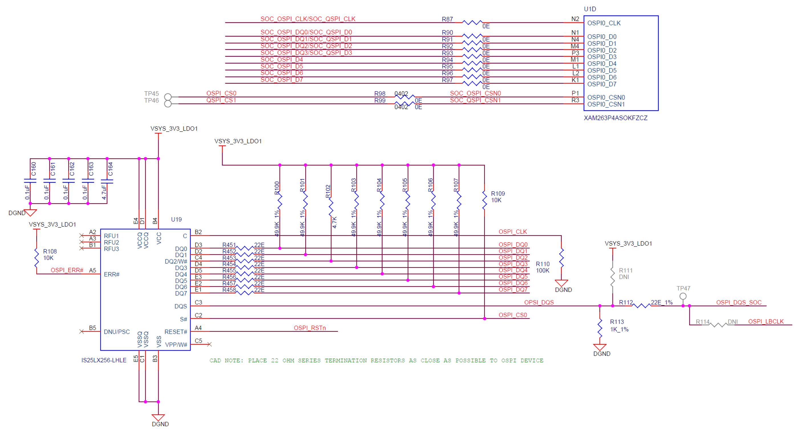
The OSPI Flash memory interface is the primary bootloader memory location for the AM263P MCU and the QSPI Flash memory interface is the primary bootloader memory location for the AM263x MCU. For a full description of boot ROM execution, including OSPI and QSPI boot information, see the AM263x Sitara™ Microcontroller Technical Reference Manual and AM263Px Sitara™ Microcontroller Technical Reference Manual. The excerpt from Figure 5-4 shows the implementation of the QSPI NOR flash interface from the LP-AM263 LaunchPad design. The excerpt from Figure 5-5 shows the implementation of the OSPI NOR flash interface on the TMDSCNCD263P AM263Px controlCard design.
 Figure 5-4 Example AM263x QSPI Controller
and NOR Flash Memory Schematic
  Figure 5-5 Example AM263Px OSPI
Controller and NOR Flash Memory Schematic
 To control OSPI/QSPI bus transition overshoot and undershoot, include the following series termination resistors close to the OSPI/QSPI memory pins and the AM263x or AM263Px BGA.
- Series termination at the AM263x or AM263Px MCU, transmit side of QSPI0_CLK, and QSPI0_CS[1:0]
- Series termination at OSPI/QSPI memory side of OSPI0_D[7:0] or QSPI0_D[3:0]
For recommended series termination resistor placement, see Figure 5-7.
The OSPI_D[7:1] and QSPI_D[3:1] bits of the interface are used as a read interface, so series termination at the memory side of the bus are used. OSPI/QSPI_D0 may benefit from termination at both the MCU side and the OSPI/QSPI memory side of the bus since is used as both a single-mode write and part of single-mode and octal/quad-mode reads. However, placement of additional termination on both sides of this bus may be difficult to achieve from a PCB floor-planning perspective. The termination scheme presented here should be used as a minimum recommendation. For more details on termination requirements, see Section 8.
Pull resistors are also also necessary on the OSPI/QSPI clock, chip-select and data lines. Include the following pull resistors on the QSPI signals. Different QSPI memory may have different pull-up/down requirements depending on the specific memory and application requirements. These pull resistor recommendations are based on the implementation of the S25FL128x memory used on the LP-AM263 design. To confirm all pin memory configuration details, see the device-specific QSPI Flash memory data sheet.
- QSPI_CLK, QSPI_CS[1:0], and QSPI_D[1:0] - include 100 kohm pull-up to VDDS33 IO suppply
- QSPI_D[2] - 10 kohm pull-up to VDDS33 IO supply. This disables write-protect mode on the S25FL128 flash memories.
- QSPI_D[3] - 10 kohm pull-up to VDDS33 IO supply. This disables hold mode on the S25FL128 flash memories
- OSPI_CLK - include 100kohm pull-down to GND
- OSPI_CS - 10kohm pull-up to VDDS33 IO supply
- OSPI_DQS - 1k pull-down to GND
- OSPI_D[2] - 4.7kohm pull-up to VDDS33 IO supply. This disables write-protect mode on the IS25LX256 flash memories
- OSPI_D[1:0] and OSPI_D[7:3] - 49.9kohm pull-up to VDDS33 IO supply
Stronger pull-up resistors are used to disable write-protect and hold modes by default. Weaker pull-up resistors are used to keep the lines at valid logic levels between transactions. Pull resistors should be placed close to the OSPI/QSPI memory pins to prevent any additional routing stubs from being formed.
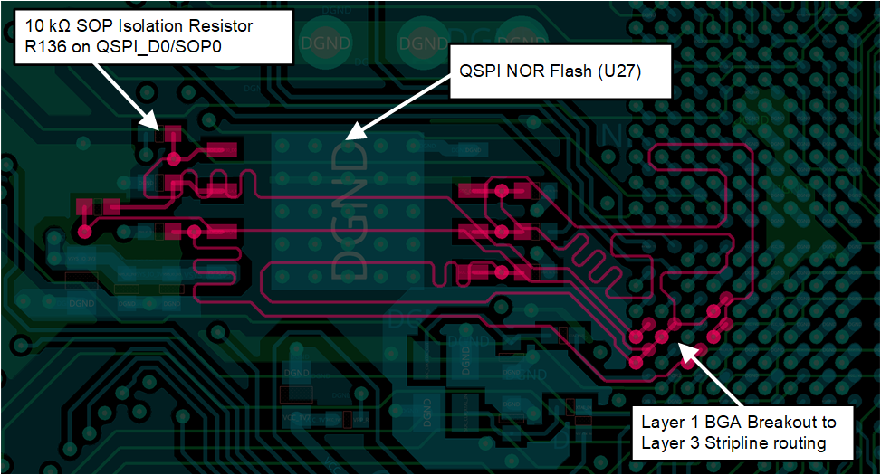
 Figure 5-6 Excerpt From LP-AM263
Launchpad Layout – Highlighting SOP0/QSPI_D0 Path and SOP Isolation
Resistor
Figure 5-6 Excerpt From LP-AM263
Launchpad Layout – Highlighting SOP0/QSPI_D0 Path and SOP Isolation
ResistorAdditional routing guidelines for the QSPI memory interface are provided in Figure 5-7 and Table 5-2. These should be used as maximum routing delay and skew match limits. The QSPI memory should be placed close to the AM263x or AM263Px BGA footprint as possible. This allows for routing that maximizes the delay margins and skew margins and minimizes transmission-line effects.
 Figure 5-7 AM263x or AM263Px QSPI -
Routing Rules Diagram
Figure 5-7 AM263x or AM263Px QSPI -
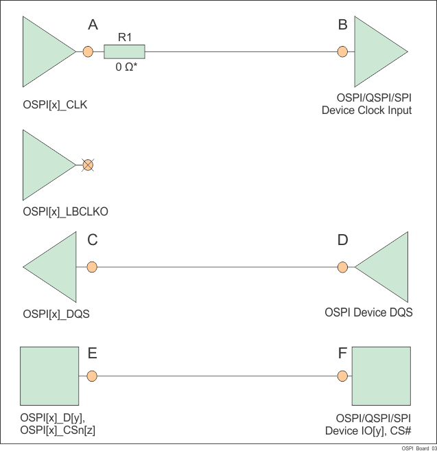
Routing Rules DiagramAdditional routing guidelines for the OSPI memory interface are provided in Figure 5-8 and Table 5-3. These should be used as maximum routing delay and skew match limits. The OSPI memory should be placed close to the AM263Px BGA footprint as possible. This allows for routing that maximizes the delay margins and skew margins and minimizes transmission-line effects.
 Figure 5-8 AM263Px OSPI - Routing Rules
Diagram
Figure 5-8 AM263Px OSPI - Routing Rules
Diagram| Spec No. | Specification | Value | Unit |
|---|---|---|---|
| 1 | QSPI_CLK, QSPI_CS0, QSPI_D[3:0] maximum delay | 450 | ps |
| 2 | QSPI_CLK to QSPI_D[3:0] maximum skew | 50 | ps |
| 3 | Approximate maximum routing distances | 3214 | mils |
| 4 | Approximate maximum routing skew | 357 | mils |
| 5 | A series termination resistor (R1 in diagram above) should be placed close to the QSPI_CLK transmit pin of the AM263x to control rise-time and reflections of the clock line. | Variable, 0 to 40 | Ω |
| 6 | A series termination resistor (R2 in diagram above) should be placed close to the QSPI data pins of the attached memory to control rise-time and reflections of the data lines. | Variable, 0 to 40 | Ω |
| Spec No. | Specification | Value | Unit |
|---|---|---|---|
| 1 | OSPI_CLK, OSPI_CS0, OSPI_D[7:0] maximum delay | 450 | ps |
| 2 | OSPI_CLK to OSPI_D[7:0] and OSPI_CSn maximum skew | 60 | ps |
| 3 | OSPI_CLK to OSPI_DQS maximum skew | 30 | ps |
| 4 | Approximate maximum routing distances | 3214 | mils |
| 5 | OSPI_CLK to OSPI_D[7:0] and OSPI_CSn approximate maximum routing skew | 429 | mils |
| 6 | OSPI_CLK to OSPI_DQS approximate maximum routing skew | 214 | mils |
| 7 | A series termination resistor (R1 in diagram above) should be placed close to the OSPI_CLK transmit pin of the AM263Px to control rise-time and reflections of the clock line. | Variable, 0 to 40 | Ω |
| 8 | Series termination resistor should be placed close to the OSPI data pins of the attached memory and the AM263Px device to control rise-time and reflections of the data lines. | Variable, 0 to 40 | Ω |