SPRAC21A June   2016  – June 2019 OMAP-L132 , OMAP-L138 , TDA2E , TDA2EG-17 , TDA2HF , TDA2HG , TDA2HV , TDA2LF , TDA2P-ABZ , TDA2P-ACD , TDA2SA , TDA2SG , TDA2SX , TDA3LA , TDA3LX , TDA3MA , TDA3MD , TDA3MV


  1.   TDA2xx and TDA2ex Performance
    1.     Trademarks
    2. SoC Overview
      1. 1.1 Introduction
      2. 1.2 Acronyms and Definitions
      3. 1.3 TDA2xx and TDA2ex System Interconnect
      4. 1.4 Traffic Regulation Within the Interconnect
        1. 1.4.1 Bandwidth Regulators
        2. 1.4.2 Bandwidth Limiters
        3. 1.4.3 Initiator Priority
      5. 1.5 TDA2xx and TDA2ex Memory Subsystem
        1. 1.5.1 Controller/PHY Timing Parameters
        2. 1.5.2 Class of Service
        3. 1.5.3 Prioritization Between DMM/SYS PORT or MPU Port to EMIF
      6. 1.6 TDA2xx and TDA2ex Measurement Operating Frequencies
      7. 1.7 System Instrumentation and Measurement Methodology
        1. 1.7.1 GP Timers
        2. 1.7.2 L3 Statistic Collectors
    3. Cortex-A15
      1. 2.1 Level1 and Level2 Cache
      2. 2.2 MMU
      3. 2.3 Performance Control Mechanisms
        1. 2.3.1 Cortex-A15 Knobs
        2. 2.3.2 MMU Page Table Knobs
      4. 2.4 Cortex-A15 CPU Read and Write Performance
        1. 2.4.1 Cortex-A15 Functions
        2. 2.4.2 Setup Limitations
        3. 2.4.3 System Performance
          1. 2.4.3.1 Cortex-A15 Stand-Alone Memory Read, Write, Copy
          2. 2.4.3.2 Results
    4. System Enhanced Direct Memory Access (System EDMA)
      1. 3.1 System EDMA Performance
        1. 3.1.1 System EDMA Read and Write
        2. 3.1.2 System EDMA Results
      2. 3.2 System EDMA Observations
    5. DSP Subsystem EDMA
      1. 4.1 DSP Subsystem EDMA Performance
        1. 4.1.1 DSP Subsystem EDMA Read and Write
        2. 4.1.2 DSP Subsystem EDMA Results
      2. 4.2 DSP Subsystem EDMA Observations
    6. Embedded Vision Engine (EVE) Subsystem EDMA
      1. 5.1 EVE EDMA Performance
        1. 5.1.1 EVE EDMA Read and Write
        2. 5.1.2 EVE EDMA Results
      2. 5.2 EVE EDMA Observations
    7. DSP CPU
      1. 6.1 DSP CPU Performance
        1. 6.1.1 DSP CPU Read and Write
        2. 6.1.2 Code Setup
          1. 6.1.2.1 Pipeline Copy
          2. 6.1.2.2 Pipeline Read
          3. 6.1.2.3 Pipeline Write
          4. 6.1.2.4 L2 Stride-Jmp Copy
          5. 6.1.2.5 L2 Stride-Jmp Read
          6. 6.1.2.6 L2 Stride-Jmp Write
      2. 6.2 DSP CPU Observations
      3. 6.3 Summary
    8. Cortex-M4 (IPU)
      1. 7.1 Cortex-M4 CPU Performance
        1. 7.1.1 Cortex-M4 CPU Read and Write
        2. 7.1.2 Code Setup
        3. 7.1.3 Cortex-M4 Functions
        4. 7.1.4 Setup Limitations
      2. 7.2 Cortex-M4 CPU Observations
        1. 7.2.1 Cache Disable
        2. 7.2.2 Cache Enable
      3. 7.3 Summary
    9. USB IP
      1. 8.1 Overview
      2. 8.2 USB IP Performance
        1. 8.2.1 Test Setup
        2. 8.2.2 Results and Observations
        3. 8.2.3 Summary
    10. PCIe IP
      1. 9.1 Overview
      2. 9.2 PCIe IP Performance
        1. 9.2.1 Test Setup
        2. 9.2.2 Results and Observations
    11. 10 IVA-HD IP
      1. 10.1 Overview
      2. 10.2 H.264 Decoder
        1. 10.2.1 Description
        2. 10.2.2 Test Setup
        3. 10.2.3 Test Results
      3. 10.3 MJPEG Decoder
        1. 10.3.1 Description
        2. 10.3.2 Test Setup
        3. 10.3.3 Test Results
    12. 11 MMC IP
      1. 11.1 MMC Read and Write Performance
        1. 11.1.1 Test Description
        2. 11.1.2 Test Results
      2. 11.2 Summary
    13. 12 SATA IP
      1. 12.1 SATA Read and Write Performance
        1. 12.1.1 Test Setup
        2. 12.1.2 Observations
          1. 12.1.2.1 RAW Performance
          2. 12.1.2.2 SDK Performance
      2. 12.2 Summary
    14. 13 GMAC IP
      1. 13.1 GMAC Receive/Transmit Performance
        1. 13.1.1 Test Setup
        2. 13.1.2 Test Description
          1. 13.1.2.1 CPPI Buffer Descriptors
        3. 13.1.3 Test Results
          1. 13.1.3.1 Receive/Transmit Mode (see )
          2. 13.1.3.2 Receive Only Mode (see )
          3. 13.1.3.3 Transmit Only Mode (see )
      2. 13.2 Summary
    15. 14 GPMC IP
      1. 14.1 GPMC Read and Write Performance
        1. 14.1.1 Test Setup
          1. 14.1.1.1 NAND Flash
          2. 14.1.1.2 NOR Flash
        2. 14.1.2 Test Description
          1. 14.1.2.1 Asynchronous NAND Flash Read/Write Using CPU Prefetch Mode
          2. 14.1.2.2 Asynchronous NOR Flash Single Read
          3. 14.1.2.3 Asynchronous NOR Flash Page Read
          4. 14.1.2.4 Asynchronous NOR Flash Single Write
        3. 14.1.3 Test Results
      2. 14.2 Summary
    16. 15 QSPI IP
      1. 15.1 QSPI Read and Write Performance
        1. 15.1.1 Test Setup
        2. 15.1.2 Test Results
        3. 15.1.3 Analysis
          1. 15.1.3.1 Theoretical Calculations
          2. 15.1.3.2 % Efficiency
      2. 15.2 QSPI XIP Code Execution Performance
      3. 15.3 Summary
    17. 16 Standard Benchmarks
      1. 16.1 Dhrystone
        1. 16.1.1 Cortex-A15 Tests and Results
        2. 16.1.2 Cortex-M4 Tests and Results
      2. 16.2 LMbench
        1. 16.2.1 LMbench Bandwidth
          1. 16.2.1.1 TDA2xx and TDA2ex Cortex-A15 LMbench Bandwidth Results
          2. 16.2.1.2 TDA2xx and TDA2ex Cortex-M4 LMBench Bandwidth Results
          3. 16.2.1.3 Analysis
        2. 16.2.2 LMbench Latency
          1. 16.2.2.1 TDA2xx and TDA2ex Cortex-A15 LMbench Latency Results
          2. 16.2.2.2 TDA2xx and TDA2ex Cortex-M4 LMbench Latency Results
          3. 16.2.2.3 Analysis
      3. 16.3 STREAM
        1. 16.3.1 TDA2xx and TDA2ex Cortex-A15 STREAM Benchmark Results
        2. 16.3.2 TDA2xx and TDA2ex Cortex-M4 STREAM Benchmark Results
    18. 17 Error Checking and Correction (ECC)
      1. 17.1 OCMC ECC Programming
      2. 17.2 EMIF ECC Programming
      3. 17.3 EMIF ECC Programming to Starterware Code Mapping
      4. 17.4 Careabouts of Using EMIF ECC
        1. 17.4.1 Restrictions Due to Non-Availability of Read Modify Write ECC Support in EMIF
          1. 17.4.1.1 Un-Cached CPU Access of EMIF
          2. 17.4.1.2 Cached CPU Access of EMIF
          3. 17.4.1.3 Non CPU Access of EMIF Memory
          4. 17.4.1.4 Debugger Access of EMIF via the Memory Browser/Watch Window
          5. 17.4.1.5 Software Breakpoints While Debugging
        2. 17.4.2 Compiler Optimization
        3. 17.4.3 Restrictions Due to i882 Errata
        4. 17.4.4 How to Find Who Caused the Unaligned Quanta Writes After the Interrupt
      5. 17.5 Impact of ECC on Performance
    19. 18 DDR3 Interleaved vs Non-Interleaved
      1. 18.1 Interleaved versus Non-Interleaved Setup
      2. 18.2 Impact of Interleaved vs Non-Interleaved DDR3 for a Single Initiator
      3. 18.3 Impact of Interleaved vs Non-Interleaved DDR3 for Multiple Initiators
    20. 19 DDR3 vs DDR2 Performance
      1. 19.1 Impact of DDR2 vs DDR3 for a Single Initiator
      2. 19.2 Impact of DDR2 vs DDR3 for Multiple Initiators
    21. 20 Boot Time Profile
      1. 20.1 ROM Boot Time Profile
      2. 20.2 System Boot Time Profile
    22. 21 L3 Statistics Collector Programming Model
    23. 22 Reference
  2.   Revision History

Impact of Interleaved vs Non-Interleaved DDR3 for Multiple Initiators

To understand the total available DDR bandwidth of the system for the interleaved versus non-interleaved mode of operation, it is required to have a multi-initiator test. In this synthetic test, the following initiators are used for the interleaved versus non-interleaved case. The DSS reporting an Underflow error was used as a reference point to know when the DDR bandwidth is maximized out in the system.

NOTE

In the current experiment for the non-interleaved case, the data is not routed through EMIF2 and the system is assumed to be a single, 32-bit DDR system.

Non-Interleaved initiators:

  • IVAHD: Executing 1080p60 decode
  • BB2D: Executing 1280x720 NV12 3 frame overlay
  • DSP1 EDMA single TC
  • DSS 3 VID + 1 GFX pipe: 2 VID pipes 720p ARGB8888, 1VID + 1 GFX RGB888

Interleaved initiators:

  • IVAHD: Executing 1080p60 decode
  • BB2D: Executing 1280x720 NV12 3 frame overlay
  • DSP1 EDMA single TC
  • DSS 3 VID + 1 GFX pipe: 2 VID pipes 720p ARGB8888, 1VID + 1 GFX RGB888
  • DSP2 EDMA two TC
  • System EDMA two TC

The throughput is measured using statistic collectors available in the L3 at the EMIF1_probe and EMIF2_probe as shown in Figure 54. The statistic collector registers are read every 100 µs for 5 seconds and the bandwidth data is obtained by dividing the number of bytes transferred in 100 µs divided by 100 µs.
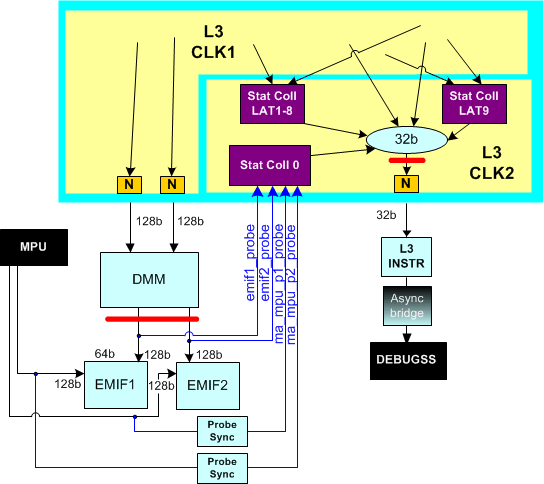
l3_statcoll_emif1_emif2_probe_mechanism_sprac21.gifFigure 54. L3 STATCOLL EMIF1 and EMIF2 PROBE Mechanism

The ideal throughput for DDR3 running at 532 MHz is:

  • For the non-Interleaved case, 532 MHz × 4 bytes × 2 = 4256 MB/s
  • For the interleaved case, (Non-Interleaved value × 2) = 8512 MB/s

Table 91 shows that when the EMIF FIFOs are fully occupied then the system can expect a 10-15% boost in performance by configuring the EMIFs in interleaved mode versus a non-interleaved mode.

Also note that this is a synthetic test to measure the maximized out EMIF throughput. When executing a real system use-case, you can expect around 55-60% DDR utilization.

Table 91. Impact of Interleaved vs Non-Interleaved DDR3 for Multiple Initiators

Non-Interleaved (One 32-Bit Memory) Interleaved (Two 32-Bit Memory)
EMIF1 Bandwidth EMIF2 Bandwidth (No Traffic to EMIF2) Total EMIF1 Bandwidth EMIF2 Bandwidth Total
Maximum Bandwidth (MB/s) 3121.60 NA 3121.60 3650.88 3642.88 7293.76
Average Bandwidth (MB/s) 2458.25 NA 2458.25 3035.51 3045.00 6080.51
Maximum DDR Utilization 73% NA 73% 86% 86% 86%
Average DDR Utilization 58% NA 58% 71% 72% 71%