SPRACP3C November 2019 – December 2021 AWR6843 , AWR6843AOP , IWR1443 , IWR1642 , IWR6443 , IWR6843 , IWR6843AOP
- Trademarks
- 1Introduction
- 2Typical Certification Procedure
- 3Regulatory Compliance Overview
- 4Tools and Setup
- 5Common Issues and Resolutions
- 6References
- 7Revision History
5.3.2.1 Hardware Measures
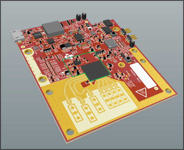
- The shield or absorber should be placed as shown in Figure 5-3 and Figure 5-4.
- Applicable mmwave devices, decoupliing caps, crystal, and the surrounding PCB area should be covered by shield or absorber.
- The shield should be well grounded, covering the components of interest, and absorbers should be properly adhered to PCB and components of interest.
- Ensure the height of the shield from the PCB is greater than or equals to 2mm above the RF traces; otherwise the RF transmission lines may couple with the shield and RF matching might get disturbed. Manufacturing tolerances, wear and tear, shield assembly, and so forth must be considered so that a 2-mm+ height from the board is always maintained.
- When using an RF absorber, the antenna should not be covered; the absorber should be placed such that it does not go beyond the edge of the IC on the areas with the TX and RX traces
- Example of an absorber used to suppress the emission is Cuming Microwave (GDX/PPGA 0.03").

All RF traces should be
at least 2 mm away from shielding cover.
Figure 5-3 Shield Placement Figure 5-4 RF Absorber Placement