SPRACW5A April 2021 – December 2021 TMS320F2800132 , TMS320F2800133 , TMS320F2800135 , TMS320F2800137 , TMS320F280021 , TMS320F280021-Q1 , TMS320F280023 , TMS320F280023-Q1 , TMS320F280023C , TMS320F280025 , TMS320F280025-Q1 , TMS320F280025C , TMS320F280025C-Q1 , TMS320F280033 , TMS320F280034 , TMS320F280034-Q1 , TMS320F280036-Q1 , TMS320F280036C-Q1 , TMS320F280037 , TMS320F280037-Q1 , TMS320F280037C , TMS320F280037C-Q1 , TMS320F280038-Q1 , TMS320F280038C-Q1 , TMS320F280039 , TMS320F280039-Q1 , TMS320F280039C , TMS320F280039C-Q1 , TMS320F280040-Q1 , TMS320F280040C-Q1 , TMS320F280041 , TMS320F280041-Q1 , TMS320F280041C , TMS320F280041C-Q1 , TMS320F280045 , TMS320F280048-Q1 , TMS320F280048C-Q1 , TMS320F280049 , TMS320F280049-Q1 , TMS320F280049C , TMS320F280049C-Q1 , TMS320F28075 , TMS320F28075-Q1 , TMS320F28076 , TMS320F28374D , TMS320F28374S , TMS320F28375D , TMS320F28375S , TMS320F28375S-Q1 , TMS320F28376D , TMS320F28376S , TMS320F28377D , TMS320F28377D-EP , TMS320F28377D-Q1 , TMS320F28377S , TMS320F28377S-Q1 , TMS320F28378D , TMS320F28378S , TMS320F28379D , TMS320F28379D-Q1 , TMS320F28379S , TMS320F28384D , TMS320F28384D-Q1 , TMS320F28384S , TMS320F28384S-Q1 , TMS320F28386D , TMS320F28386D-Q1 , TMS320F28386S , TMS320F28386S-Q1 , TMS320F28388D , TMS320F28388S , TMS320F28P650DH , TMS320F28P650DK , TMS320F28P650SH , TMS320F28P650SK , TMS320F28P659DH-Q1 , TMS320F28P659DK-Q1 , TMS320F28P659SH-Q1
- Trademarks
- 1Introduction
- 2ACI Motor Control Benchmark Application
- 3Real-time Benchmark Data Analysis
-
4C2000 Value Proposition
- 4.1 Efficient Signal Chain Execution With Better Real-Time Response Than Higher Computational MIPS Devices
- 4.2 Excellent Real-Time Interrupt Response With Low Latency
- 4.3 Tight Peripheral Integration That Scales Applications With Large Number of Peripheral Accesses
- 4.4 Best in Class Trigonometric Math Engine
- 4.5 Versatile Performance Boosting Compute Engine (CLA)
- 4.6 Deterministic Execution due to Low Execution Variance
- 5Summary
- 6References
- 7Revision History
3.2 Peripheral Access
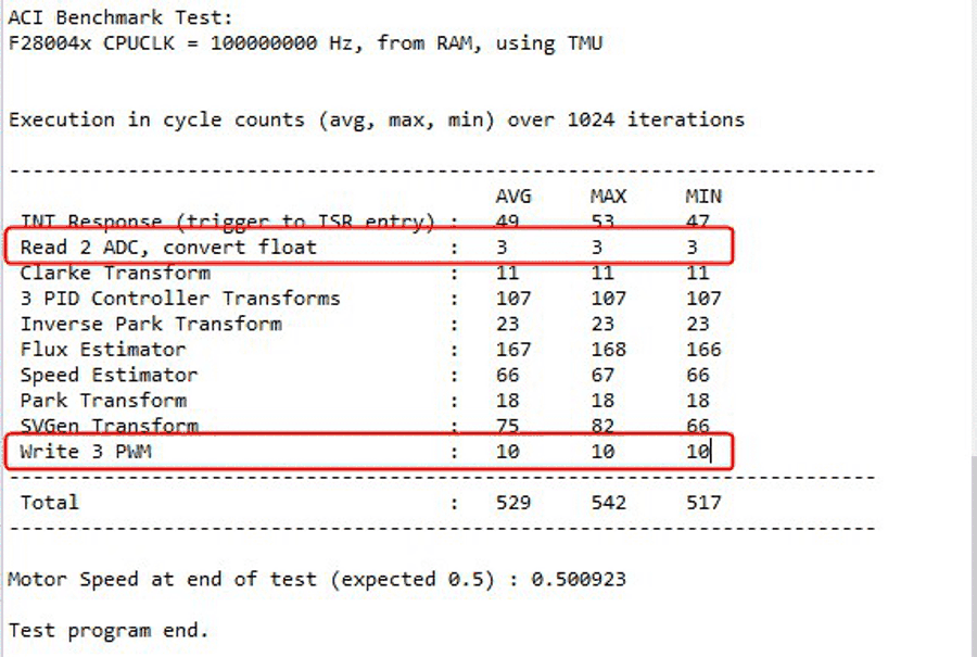
The ACI real-time benchmark has two peripheral access responses: ADC read and convert to float as well as PWM write. For the response times for each of these operations, see Figure 3-3.
 Figure 3-3 ACI Motor Benchmark Peripheral
Access Benchmark Data
Figure 3-3 ACI Motor Benchmark Peripheral
Access Benchmark DataIn this particular implementation, only two ADC inputs are being read and three PWM outputs are being written. As can be seen in Table 3-2, in other practical applications involving motor control or digital power the number of these operations can be larger and can have a bigger impact on the execution duration of a control application.
In the C2000 architecture the CPU is closely integrated with the peripherals and the instruction set architecture is optimized for floating point operations. From the benchmark data in Table 3-3, it can be derived that it takes only ~2 cycles to read one ADC input and convert it to float and just ~3 cycles to write one PWM output. As such, C2000 architecture can effectively scale to applications with large number of peripheral accesses.
Table 3-2 captures the estimated cycles for some real control applications based on the benchmarking data.
| Application | Number of ADC Reads | Number of PWM Writes | Estimated Total Cycles |
|---|---|---|---|
3 Phase AC motor control application |
7 | 3 | 23 (1) |
| Totem-pole PFC digital power application |
10 |
9 |
47 (2) |